Brief Introduction to Lithography in Semiconductor Manufacturing: Lithography is a fundamental process in semiconductor manufacturing that enables the creation of intricate patterns on silicon wafers, which are essential for producing microchips and integrated circuits (ICs). This process is central to the advancement of electronic devices, powering everything from smartphones to supercomputers.
The Role of Lithography in Semiconductor Manufacturing
In the semiconductor industry, lithography is akin to printing circuits on silicon wafers. It involves transferring a pattern from a photomask onto a substrate using light. This patterned substrate forms the basis of the tiny electronic circuits that power modern devices. As semiconductor technology has advanced, the ability to create smaller and more complex patterns has become critical for enhancing performance and reducing the size of electronic components.
Basic Principles of Lithography
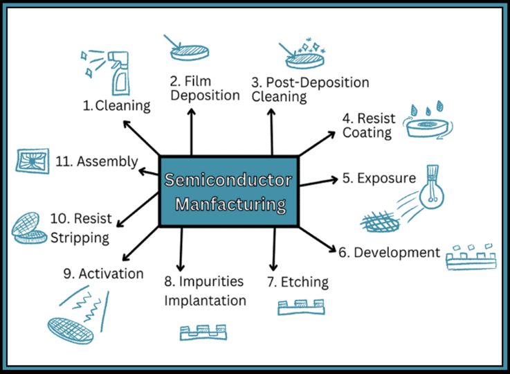
The lithographic process can be broken down into several key steps (Lithography in Semiconductor Manufacturing):
- Coating the Wafer: The silicon wafer is coated with a light-sensitive material called a photoresist.
- Exposure: A photomask, which contains the desired circuit pattern, is aligned over the wafer. Ultraviolet (UV) light is then shone through the mask, transferring the pattern onto the photoresist.
- Developing: The wafer is developed, removing the exposed or unexposed photoresist (depending on whether a positive or negative photoresist is used), thus revealing the pattern on the wafer.
- Etching: The exposed areas of the wafer are etched away, creating the physical structures of the circuit.
- Cleaning: Residual photoresist is removed, leaving behind the patterned wafer.
This process is repeated multiple times with different masks and layers to build up complex multi-layered circuits.
Evolution of Lithography Techniques
Lithography has evolved significantly since its inception. Early techniques used visible light and were limited by the wavelength of light, which constrained the minimum feature size that could be achieved. As the demand for smaller and more powerful chips grew, the industry transitioned to shorter wavelengths of light, such as deep ultraviolet (DUV) lithography.
However, even DUV lithography faced limitations as feature sizes continued to shrink. This led to the development of advanced techniques like immersion lithography, which uses a liquid medium to increase the numerical aperture of the system, allowing for finer resolution.
Challenges in Traditional Lithography
As the semiconductor industry pushes toward smaller nodes, traditional lithography faces several challenges:
- Resolution Limits: The diffraction limit of light constrains the smallest feature size that can be reliably printed.
- Complexity and Cost: Advanced lithographic techniques require sophisticated equipment and processes, driving up costs.
- Defects and Yield: Smaller feature sizes increase the likelihood of defects, impacting yield and reliability.
These challenges have spurred the development of next-generation lithographic techniques, such as Extreme Ultraviolet Lithography (EUVL), which uses even shorter wavelengths to overcome the limitations of traditional methods.
Lithography is a cornerstone of semiconductor manufacturing, enabling the creation of the intricate patterns that form the basis of modern electronic devices. While traditional lithographic techniques have served the industry well, the relentless drive for smaller, faster, and more efficient chips continues to push the boundaries of what is possible. This ongoing evolution underscores the importance of lithography in the ever-advancing field of semiconductor technology.
The Importance of Lithography in the Production of Microchips
Lithography is an indispensable process in the production of microchips, playing a critical role in the semiconductor manufacturing industry. It is through lithography that the intricate patterns of circuits are etched onto silicon wafers, forming the backbone of all modern electronic devices. The significance of lithography in microchip production cannot be overstated, as it directly impacts the performance, size, and cost of semiconductor devices.
The Core of Semiconductor Manufacturing
Lithography is often described as the core of semiconductor manufacturing because it defines the geometries of the integrated circuits (ICs) that power everything from computers and smartphones to medical devices and automotive systems. The process involves using light to transfer a geometric pattern from a photomask to a light-sensitive chemical photoresist on the silicon wafer. This patterned photoresist serves as a stencil for subsequent processes, such as etching and doping, which create the physical structures of the IC.
Enabling Miniaturization and Performance Improvements
One of the primary drivers of progress in the semiconductor industry is the relentless pursuit of miniaturization, often referred to as Moore’s Law. This principle, coined by Intel co-founder Gordon Moore, predicts that the number of transistors on a microchip will double approximately every two years, leading to exponential increases in computing power and efficiency. Lithography is a key enabler of this trend.
As lithographic techniques have advanced, they have allowed for the production of smaller and smaller features on microchips. The ability to pattern tiny transistors with dimensions measured in nanometers has led to significant improvements in chip performance, power consumption, and density. These advancements are crucial for the development of cutting-edge technologies, such as artificial intelligence, high-speed computing, and next-generation communication networks.
Precision and Complexity in Chip Design
Modern microchips are incredibly complex, containing billions of transistors and multiple layers of interconnected circuits. Lithography must achieve an extraordinary level of precision to accurately reproduce these intricate designs on a wafer. Any deviation or defect can result in faulty chips, affecting the yield and reliability of semiconductor products.
To meet these demands, semiconductor manufacturers use advanced lithographic equipment and techniques. For instance, deep ultraviolet (DUV) lithography and extreme ultraviolet (EUV) lithography utilize shorter wavelengths of light to achieve finer resolutions. Immersion lithography, another advanced technique, involves submerging the wafer in a liquid medium to enhance the resolution further.
Cost Efficiency and Mass Production
The economics of semiconductor manufacturing are heavily influenced by lithography. The cost of lithographic equipment and materials represents a significant portion of the overall cost of chip production. However, advances in lithography also drive cost efficiency by enabling higher yields and reducing the number of defective chips.
Moreover, lithography’s ability to produce chips at scale is vital for meeting the global demand for electronic devices. High-throughput lithography systems can process hundreds of wafers per hour, each containing thousands of individual chips. This mass production capability is essential for maintaining the supply chain and supporting the rapid growth of technology markets.
Also, Read: What is Edge Computing? Complete Guide
Lithography and Innovation
Innovation in lithography is a continuous process, with ongoing research and development aimed at overcoming current limitations and pushing the boundaries of what is possible. As the industry moves towards even smaller nodes, new challenges arise, such as managing patterning defects, improving photoresist materials, and increasing light source power.
Collaborative efforts among semiconductor companies, research institutions, and equipment manufacturers are driving the next generation of lithographic technologies. These innovations promise to sustain the momentum of Moore’s Law and open up new possibilities for semiconductor applications.
Introduction to Extreme Ultraviolet Lithography (EUVL)
Extreme Ultraviolet Lithography (EUVL) is a cutting-edge technology that represents a significant leap forward in the field of semiconductor manufacturing. As the demand for smaller, faster, and more efficient microchips continues to grow, traditional lithographic methods are reaching their physical and technical limits. EUVL emerges as a solution to these challenges, enabling the production of next-generation semiconductor devices with unprecedented precision and scalability.
The Basics of Lithography
To appreciate the impact of EUVL, it’s important to understand the basics of lithography. Lithography is a process used in semiconductor fabrication to transfer intricate circuit patterns onto a silicon wafer. This involves using light to project the pattern from a photomask onto a photosensitive layer on the wafer. The patterned layer then guides subsequent etching and deposition steps to create the physical structures of the microchip.
The Need for Advanced Lithography Techniques
As semiconductor technology advances, the features on microchips must become increasingly smaller to enhance performance and reduce power consumption. Traditional lithographic techniques, such as deep ultraviolet (DUV) lithography, use light with wavelengths of 193 nanometers. However, these techniques are approaching their resolution limits, making it difficult to produce features smaller than 10 nanometers.
Enter Extreme Ultraviolet Lithography
EUVL addresses these limitations by using extreme ultraviolet (EUV) light with a wavelength of 13.5 nanometers—much shorter than the light used in DUV lithography. This shorter wavelength allows EUVL to achieve much finer resolutions, enabling the creation of smaller and more densely packed features on microchips. This capability is critical for continuing the trend of miniaturization in semiconductor devices, often referred to as Moore’s Law.
Extreme Ultraviolet Lithography (EUVL) is a state-of-the-art technology used in the semiconductor manufacturing process to create extremely fine patterns on silicon wafers. These patterns form the circuits of microchips, which are integral to all modern electronic devices. The basic working principle of EUVL involves several complex steps and components, all designed to harness and manipulate extreme ultraviolet (EUV) light with a wavelength of 13.5 nanometers. Here is an overview of the key elements and processes involved in EUVL:
1. Generation of EUV Light
Light Source:
Laser-Produced Plasma (LPP) Source:
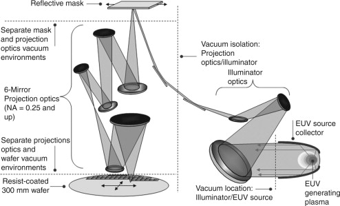
- The EUV light source is a critical component of the EUVL process. It begins with generating extreme ultraviolet light at a wavelength of 13.5 nanometers. This is achieved using a laser-produced plasma (LPP) source. A high-powered laser is directed at tin droplets, creating a plasma that emits EUV radiation. The generation of a stable and powerful EUV light source is one of the most challenging aspects of EUVL.
2. EUV Optics
Reflective Optics:
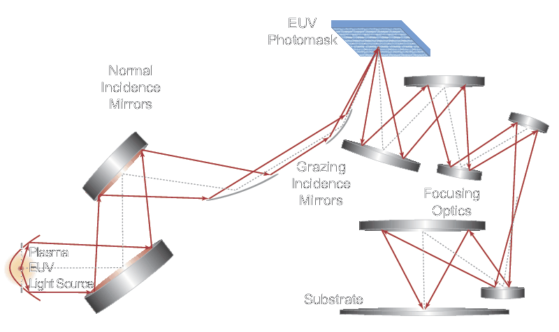
- Unlike traditional lithography, which uses lenses to focus light, EUVL relies on reflective optics. This is because EUV light is absorbed by most materials, including air. Therefore, the entire EUVL process occurs in a vacuum, and mirrors made of multilayer coatings are used to reflect and focus the EUV light onto the wafer.
Multilayer Mirrors:
- These mirrors are made by stacking thin layers of materials with differing refractive indices, designed to reflect EUV light efficiently. The precision in the layering is crucial to ensure the correct reflection and focusing of the light.
Also, Read: What is Wireless Power Transfer (WPT) Technology?
3. Photomask
EUV Masks:
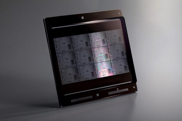
- A photomask, or reticle, is used to carry the pattern of the circuit to be printed onto the wafer. The mask for EUVL is significantly different from those used in traditional lithography. It is made with reflective materials and must be free of defects to ensure accurate pattern transfer. The pattern on the mask is a negative image of the circuit that will be created on the wafer.
4. Exposure
Exposure Tool:
- The wafer is coated with a photosensitive material called a photoresist. The EUV light, carrying the pattern from the photomask, is then projected onto the photoresist-coated wafer. The areas of the photoresist exposed to the EUV light undergo chemical changes.
5. Developing the Pattern
Photoresist Development:
- After exposure, the wafer undergoes a development process. The exposed regions of the photoresist are either removed or retained, depending on whether a positive or negative photoresist is used. This development step reveals the pattern that was transferred from the photomask.
6. Etching
Etching Process:
- The developed pattern on the photoresist serves as a stencil for etching. In the etching process, chemical or plasma etchants remove the exposed parts of the wafer, transferring the pattern into the underlying material.
7. Final Processing
Cleaning and Layering:
- After etching, the remaining photoresist is stripped away, and additional layers of materials may be deposited and patterned to create the multi-layered structures of modern integrated circuits. This process of coating, exposing, developing, and etching is repeated multiple times to build the complete semiconductor device.
Defect Detection and Correction:
- Throughout the EUVL process, rigorous inspection and quality control measures are implemented to detect and correct any defects. Advanced metrology tools are used to ensure the accuracy and precision of the patterned features, which is crucial for the functionality and reliability of the final microchips.
Advantages of EUVL
- Higher Resolution: The 13.5 nm wavelength allows for the creation of much smaller features than traditional lithographic techniques, enabling the continued scaling down of semiconductor devices.
- Simplified Process: EUVL can reduce the need for multiple patterning steps required in DUV lithography, potentially simplifying the manufacturing process and improving throughput.
Challenges in EUVL
- Light Source Power: Generating a stable and powerful EUV light source is challenging and crucial for efficient production.
- Mask Defects: Producing defect-free masks that can handle the precise requirements of EUVL is complex and costly.
- Vacuum Environment: Maintaining the necessary vacuum conditions adds to the complexity and cost of the EUVL process.
Why Tin is Used in Extreme Ultraviolet (EUV) Lithography?
Tin (Sn) is used as a source material in the generation of extreme ultraviolet (EUV) light for EUV lithography, a cutting-edge technology critical for manufacturing advanced semiconductor devices. Here’s a detailed explanation of why tin is chosen for this process:
1. Optimal Emission Wavelength
13.5 nm Wavelength:
- The EUV lithography process requires light at a very specific wavelength of 13.5 nanometers (nm). Tin is particularly suitable because, when ionized, it emits strong radiation in this wavelength range. This emission is in the extreme ultraviolet spectrum, which is ideal for achieving the small feature sizes needed for advanced semiconductor nodes (e.g., 7nm, 5nm, 3nm).
2. High Conversion Efficiency
Efficient Plasma Generation:
- When tin is heated by a high-powered laser, it forms a plasma that emits EUV light efficiently. Tin has a relatively high conversion efficiency, meaning it can effectively convert the energy from the laser into EUV light. This efficiency is crucial for creating a strong and consistent EUV light source necessary for high-throughput semiconductor manufacturing.
3. Availability and Manageability
Material Availability:
- Tin is a relatively abundant and cost-effective material, making it a practical choice for use in industrial applications. Its availability ensures a steady supply for the high-volume manufacturing needs of the semiconductor industry.
Manageable Physical Properties:
- Tin’s physical properties, such as its melting and boiling points, make it manageable in the controlled environment of EUV lithography systems. It can be precisely manipulated in the form of tiny droplets to produce consistent plasma when struck by the laser.
4. Compatibility with Laser-Produced Plasma (LPP) Technology
Laser-Produced Plasma Source:
- The most common method for generating EUV light in lithography is the laser-produced plasma (LPP) technique. In this method, tin droplets are irradiated by high-energy laser pulses, creating a plasma that emits EUV light. Tin’s ability to efficiently form plasma under laser irradiation makes it compatible with this technology.

Droplet Formation and Targeting:
- Tin can be formed into small droplets that are consistently targeted by the laser pulses. This precise formation and targeting are essential for maintaining a stable and reliable EUV light source.
5. Reduction of Debris and Contamination
Low Debris Production:
- Compared to other potential materials, tin produces relatively low amounts of debris when it forms plasma. This is important because debris can contaminate the EUV optics and reduce the efficiency and lifespan of the lithography system. Effective debris management systems are in place to minimize any residual impact.
Also, Read: What is Digital Twin Technology? Complete Guide
The Wavelength of Extreme Ultraviolet Light Used in EUVL (13.5 nm): A Leap in Lithography Technology
The semiconductor industry thrives on the relentless pursuit of miniaturization and efficiency. Central to this pursuit is lithography, the process of transferring circuit patterns onto silicon wafers to create microchips. Over the decades, lithographic techniques have evolved, primarily driven by the need to produce smaller and more complex features. This evolution has culminated in the advent of Extreme Ultraviolet Lithography (EUVL), which utilizes a revolutionary wavelength of 13.5 nanometers (nm). This article delves into the significance of this wavelength, its advantages, and how it compares to previous generations of lithographic technologies.
The Evolution of Lithographic Wavelengths
Lithography has undergone several transformations, each marked by the use of progressively shorter wavelengths of light:
- G-Line and I-Line Lithography:
- Early lithographic processes used mercury lamps emitting at wavelengths of 436 nm (G-line) and 365 nm (I-line). These techniques were sufficient for manufacturing microchips with feature sizes down to about 0.8 micrometers.
- Deep Ultraviolet (DUV) Lithography:
- The next significant leap came with the introduction of DUV lithography, which employs excimer lasers emitting at 248 nm (KrF) and later 193 nm (ArF). DUV lithography enabled the production of microchips with feature sizes down to 10 nm. This technology became the workhorse of the industry, driving the exponential growth of computational power.
- Immersion Lithography:
- To further enhance the resolution, immersion lithography was developed, where a liquid (typically water) is placed between the lens and the wafer. This technique effectively increases the numerical aperture of the system, allowing for finer feature sizes using the same 193 nm light.
The Shift to Extreme Ultraviolet Lithography (EUVL)
As the industry aimed for even smaller feature sizes, the limitations of DUV lithography became apparent. The physical properties of light set a lower bound on the feature sizes that could be reliably produced. This limitation spurred the development of EUVL, which uses an extreme ultraviolet wavelength of 13.5 nm.
Why 13.5 nm?
The choice of 13.5 nm for EUVL is based on a balance of several factors:
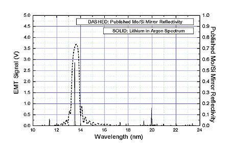
- Absorption Characteristics: At 13.5 nm, light is strongly absorbed by most materials, including air. This necessitates that EUVL be conducted in a vacuum, but it also allows for very fine patterning, as the shorter wavelength can resolve much smaller features.
- Availability of Suitable Light Sources: Generating EUV light at 13.5 nm is feasible using laser-produced plasma sources. These sources create EUV light by heating a target material, typically tin, to extreme temperatures, producing a plasma that emits EUV radiation.
- Reflective Optics: At this wavelength, conventional refractive optics are ineffective. Instead, special multilayer mirrors are used to focus and direct the EUV light. These mirrors are designed to reflect EUV light efficiently at 13.5 nm, ensuring sufficient intensity for the lithographic process.
Advantages of EUVL at 13.5 nm
The transition to 13.5 nm EUV light offers several critical advantages:
- Higher Resolution: The shorter wavelength allows for the patterning of features smaller than 10 nm, supporting the continued miniaturization of semiconductor devices.
- Simplified Process: EUVL can potentially reduce the number of patterning steps required, as it can achieve finer resolutions without the need for complex techniques like multiple patterning used in DUV lithography.
- Improved Performance: Microchips produced with EUVL can achieve higher performance and energy efficiency, which is essential for advancing technologies like artificial intelligence, 5G communications, and high-performance computing.
Challenges and Overcoming Them
Despite its advantages, EUVL at 13.5 nm presents several challenges:
- Light Source Power: Generating a powerful and stable EUV light source is difficult. The current sources are not as intense as traditional DUV lasers, which can limit throughput.
- Mask Defects: The masks used in EUVL must be nearly perfect, as any defect can be transferred to the wafer, affecting the yield.
- Material Sensitivity: The photoresists used in EUVL need to be highly sensitive to 13.5 nm light to ensure accurate patterning.
The semiconductor industry has made significant progress in addressing these challenges. Advances in light source technology, the development of defect-free masks, and new photoresist materials are steadily improving the viability and efficiency of EUVL.
Also, Read: Trends in Welding Technology
Key Differences Between EUVL and Traditional Lithography Techniques
Extreme Ultraviolet Lithography (EUVL) represents a significant advancement over traditional lithography techniques used in semiconductor manufacturing. By utilizing a much shorter wavelength of light, EUVL enables the creation of finer, more precise features on microchips. This article explores the key differences between EUVL and traditional lithography methods, highlighting the technological innovations and the challenges that come with this cutting-edge approach.
1. Wavelength of Light
Traditional Lithography:
- Traditional lithography techniques, such as Deep Ultraviolet (DUV) lithography, use light with wavelengths of 193 nanometers (nm) (ArF excimer laser) or 248 nm (KrF excimer laser). These wavelengths were adequate for producing feature sizes down to about 10 nm, but further miniaturization presented significant challenges.
EUVL:
- EUVL employs extreme ultraviolet light with a wavelength of 13.5 nm. This much shorter wavelength allows for significantly smaller feature sizes, facilitating the production of more advanced and densely packed semiconductor devices.
2. Light Source and Generation
Traditional Lithography:
- In traditional lithography, light sources such as excimer lasers (ArF and KrF) are used. These lasers are well-developed and provide stable, high-intensity light necessary for the photolithographic process.
EUVL:
- EUVL requires a completely different light source. It uses a laser-produced plasma (LPP) light source, where a high-powered laser hits a tin droplet, creating a plasma that emits EUV radiation at 13.5 nm. Generating and maintaining a stable EUV light source is one of the biggest challenges of EUVL.
3. Optical System
Traditional Lithography:
- Traditional lithography uses refractive optics (lenses) to focus and direct the light onto the wafer. These systems are well-understood and relatively easy to manufacture and maintain.
EUVL:
- EUV light is absorbed by most materials, including air and standard lenses, making refractive optics impractical. Instead, EUVL uses reflective optics, specifically multilayer mirrors, to focus and direct the light. These mirrors are complex to manufacture and require highly precise alignment and maintenance.
4. Process Environment
Traditional Lithography:
- Traditional lithography is typically performed in a cleanroom environment, but it does not require a vacuum. The process can be conducted in air or with specific gases that do not interfere with the UV light.
EUVL:
- Because EUV light is absorbed by air, EUVL must be conducted in a vacuum environment. This adds complexity and cost to the process, as maintaining a vacuum is technically demanding and requires specialized equipment.
5. Photomask Technology
Traditional Lithography:
- Photomasks used in traditional lithography are made with materials that are transparent to the wavelengths of DUV or UV light. These masks can be produced with high precision and relatively low defect rates.
EUVL:
- Photomasks for EUVL are significantly more complex. They must reflect rather than transmit light, requiring a different set of materials and manufacturing techniques. Additionally, the precision required to produce defect-free EUV masks is much higher, making them more challenging and expensive to fabricate.
6. Photoresist Materials
Traditional Lithography:
- The photoresists used in traditional lithography are well-established, with chemistries optimized for UV and DUV wavelengths. These resists are highly sensitive and can achieve the necessary resolutions for most current semiconductor devices.
EUVL:
- EUV photoresists need to be sensitive to the 13.5 nm wavelength, which presents new chemical challenges. Developing resists that can handle the high-energy EUV photons while maintaining resolution and line edge roughness is an ongoing area of research and development.
7. Cost and Infrastructure
Traditional Lithography:
- The infrastructure for traditional lithography, including equipment, materials, and processes, is well-established. The costs are high but have been optimized over decades of use.
EUVL:
- EUVL infrastructure is still being developed and optimized. The initial costs for EUV systems are extremely high, due to the complexity of the light sources, optics, vacuum environments, and masks. The industry is working to bring these costs down as the technology matures and becomes more widely adopted.
| Aspect | Traditional Lithography | EUVL |
| Wavelength of Light | 193 nm (ArF excimer laser), 248 nm (KrF excimer laser) | 13.5 nm |
| Light Source and Generation | Excimer lasers (ArF and KrF) | Laser-produced plasma (LPP) hitting tin droplets |
| Optical System | Refractive optics (lenses) | Reflective optics (multilayer mirrors) |
| Process Environment | Conducted in air or specific gases | Conducted in a vacuum environment |
| Photomask Technology | Made with materials transparent to DUV/UV light | Made with materials for reflecting EUV light, higher precision needed |
| Photoresist Materials | Optimized for UV and DUV wavelengths | Sensitive to 13.5 nm wavelength, new chemical challenges |
| Cost and Infrastructure | Established, optimized over decades | High initial costs, complex infrastructure still being optimized |
This table summarizes the key differences between traditional lithography and Extreme Ultraviolet Lithography (EUVL).
Also, Read: Trends in Electrical Cables
Materials Used in EUV Lithography
Extreme Ultraviolet Lithography (EUVL) involves various specialized materials that are crucial for generating, manipulating, and utilizing extreme ultraviolet light with a wavelength of 13.5 nanometers. Here is an overview of the key materials used in EUV lithography:
1. Light Source Materials
Tin (Sn):
- Tin is the primary material used in the generation of EUV light. It is used in the form of tiny droplets that are ionized by high-energy laser pulses to create a plasma that emits EUV radiation. Tin’s efficient emission at the 13.5 nm wavelength makes it ideal for this purpose.
2. Optical Components
Multilayer Mirrors:
- Materials: Multilayer mirrors are typically composed of alternating layers of molybdenum (Mo) and silicon (Si). Each layer is only a few nanometers thick.
- Function: These mirrors are designed to reflect EUV light efficiently. They are crucial for directing and focusing the EUV light onto the wafer because traditional lenses do not work at EUV wavelengths due to high absorption.
Reflective Coatings:
- Materials: Besides Mo/Si, other materials like ruthenium (Ru) can be used as capping layers to protect the multilayer structure from oxidation and contamination.
- Function: The reflective coatings enhance the mirror’s reflectivity and durability, ensuring consistent performance during the lithography process.
3. Photomasks (Reticles)
Mask Blanks:
- Materials: The substrate of EUV masks is usually made from low thermal expansion glass or quartz. The reflective surface consists of multilayer coatings similar to those used in mirrors, primarily Mo/Si.
- Absorbing Layer: The pattern on the mask is created using an absorber layer, typically made of materials like tantalum-based compounds (e.g., tantalum boron nitride, TaBN).
- Function: These photomasks define the circuit patterns that are projected onto the wafer. The precision and stability of these materials are critical for accurate patterning.
4. Photoresists
Chemically Amplified Resists (CARs):
- Materials: CARs typically consist of a polymer matrix and a photoacid generator (PAG). When exposed to EUV light, the PAG produces acid, which catalyzes a chemical reaction during the post-exposure bake, changing the solubility of the resist.
- Function: These resists are sensitive to EUV light and allow for the transfer of fine patterns onto the wafer. They are designed to achieve high resolution and low line-edge roughness (LER).
Metal-Containing Resists:
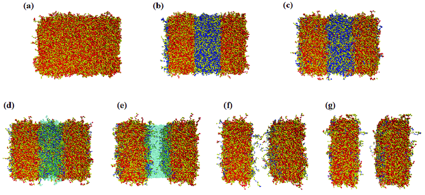
- Materials: Newer EUV resists may contain metals such as hafnium or zirconium to increase EUV absorption and enhance resolution.
- Function: These advanced resists offer improved performance for sub-10 nm patterning, providing better resolution and sensitivity.
5. Pellicles
Carbon Nanotube (CNT) Pellicles:
- Materials: Made from carbon nanotubes, which provide high transparency to EUV light, excellent mechanical strength, and thermal stability.
- Function: Pellicles protect the photomask from contamination without significantly attenuating the EUV light. Their durability and transparency are crucial for maintaining the efficiency and reliability of the lithography process.
Silicon-Based Pellicles:
- Materials: Silicon-based materials or other advanced polymers are also used for their high EUV transparency and robustness.
- Function: Similar to CNT pellicles, these materials protect the photomask while allowing sufficient EUV light transmission.
6. Other Materials
Debris Mitigation Systems:
- Materials: Components made from advanced ceramics and heat-resistant metals are used to manage and mitigate debris generated during the EUV light generation process.
- Function: These materials help protect the EUV optics and maintain the system’s cleanliness and efficiency.
Coolants and Lubricants:
- Materials: High-performance synthetic coolants and lubricants are used to manage the thermal loads and mechanical operations within EUV lithography systems.
- Function: These materials ensure stable operating temperatures and reduce wear on moving parts, enhancing the longevity and reliability of the equipment.
Also, Read: Plastic Trends in USA (Specific Use in Automotive Sector)
Recent Advancements in EUVL Technology
Extreme Ultraviolet Lithography (EUVL) has emerged as a pivotal technology in semiconductor manufacturing, enabling the production of advanced microchips with incredibly small and precise features. Despite its transformative potential, EUVL has faced numerous technical challenges since its inception. Recent advancements in EUVL technology have addressed many of these challenges, significantly improving its efficiency, reliability, and scalability. Here, we explore some of the key recent advancements in EUVL technology.
1. Enhanced EUV Light Sources
Increased Source Power:
- One of the major hurdles in EUVL has been generating a powerful and stable EUV light source. Recent advancements have focused on increasing the power of the laser-produced plasma (LPP) sources. Innovations in laser technology and the optimization of the tin droplet target have resulted in EUV sources capable of producing higher intensity light. These improvements have significantly increased the throughput of EUV systems, making them more suitable for high-volume manufacturing.
Higher Efficiency Collectors:
- Advances in the design and materials of EUV light collectors have improved their efficiency. By optimizing the multilayer coatings and the shape of the collectors, more EUV light can be captured and directed onto the wafer, enhancing the overall efficiency of the lithography process.
2. Advanced Photomasks
Defect Mitigation:
- Photomask defects have been a significant challenge in EUVL. Recent developments in mask fabrication techniques have focused on reducing defects and improving mask durability. Advanced inspection and repair tools now allow for the detection and correction of defects at the nanometer scale, ensuring higher quality masks.
Protective Pellicles:
- Protective pellicles, thin transparent membranes placed over the photomask, have been developed to prevent particle contamination. These pellicles are designed to withstand the harsh EUV environment and have become an essential component in improving the reliability and yield of EUV lithography.
3. Improved Photoresist Materials
High-Sensitivity Resists:
- The development of new photoresist materials with higher sensitivity to EUV light has been a critical advancement. These resists allow for more efficient patterning with lower doses of EUV radiation, enhancing the resolution and reducing the overall energy requirements of the process.
Chemically Amplified Resists (CARs):
- Chemically amplified resists have been optimized for EUV lithography, offering improved resolution and line edge roughness. These resists use a chemical amplification process to enhance the sensitivity and pattern fidelity, crucial for producing advanced semiconductor devices.
4. Metrology and Inspection Tools
High-Resolution Inspection:
- The precision required for EUV lithography demands advanced metrology and inspection tools. Recent advancements have led to the development of high-resolution inspection systems capable of detecting defects at the atomic scale. These systems use techniques such as scanning electron microscopy (SEM) and atomic force microscopy (AFM) to ensure the accuracy of the patterned features.
In-Line Metrology:
- The integration of in-line metrology tools into the EUV production process has improved real-time monitoring and control. These tools provide immediate feedback on the quality of the lithography process, allowing for prompt adjustments and corrections, thereby enhancing yield and reducing waste.
5. System Integration and Automation
Automated Handling Systems:
- Automation has played a significant role in advancing EUVL technology. Automated wafer handling systems have been developed to operate within the vacuum environment required for EUV lithography. These systems ensure precise and contamination-free transport of wafers, improving the overall efficiency and reliability of the process.
Integrated Process Control:
- Advanced software and control systems have been integrated into EUV lithography tools to enhance process control. These systems use machine learning and artificial intelligence to optimize the lithography parameters in real-time, leading to better performance and higher yields.
6. Collaboration and Industry Support
Consortia and Partnerships:
- Collaboration between semiconductor manufacturers, equipment suppliers, and research institutions has been crucial in advancing EUVL technology. Industry consortia such as ASML, IMEC, and SEMATECH have played a pivotal role in driving research and development efforts, sharing knowledge, and pooling resources to overcome technical challenges.
Also, Read: Safety in Cement Plants and Technology
Approaches to Overcoming Current Challenges in EUVL
Extreme Ultraviolet Lithography (EUVL) has made significant strides in semiconductor manufacturing, yet it still faces several technical challenges that need to be addressed to fully realize its potential. These challenges include issues with pellicles, resist materials, and overall process efficiency. Here, we explore the innovative approaches being taken to overcome these hurdles.
1. Enhancing Pellicle Technology
Development of Durable Pellicles:
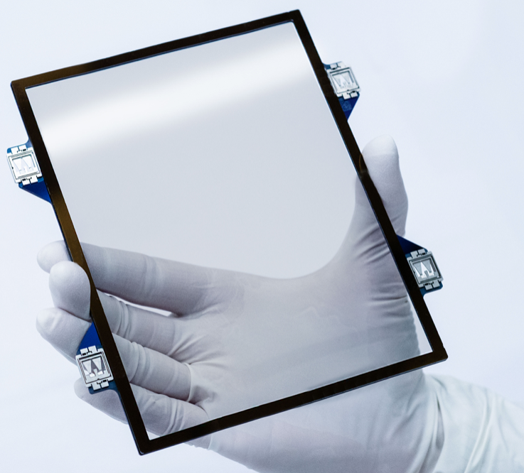
- Pellicles are crucial for protecting photomasks from contamination during the EUV lithography process. Traditional pellicles, used in older lithography techniques, are not suitable for EUV due to the high energy of EUV photons. New materials and designs are being developed to create pellicles that can withstand the intense EUV radiation while maintaining high transmission efficiency.
Advanced Materials:
- Researchers are exploring advanced materials such as silicon-based compounds and carbon nanotubes to fabricate pellicles that can endure the harsh EUV environment. These materials are designed to be thin yet robust, ensuring minimal interference with the EUV light while providing effective protection against particles.
Thermal Management:
- One of the significant challenges with EUV pellicles is managing the heat generated by the EUV light. Innovative cooling techniques and materials with high thermal conductivity are being integrated into pellicle designs to dissipate heat efficiently, preventing damage and ensuring long-term reliability.
2. Improving Resist Materials
High-Sensitivity Resists:
- EUV resists must be highly sensitive to 13.5 nm EUV light to achieve fine feature patterning. Developing resists with higher sensitivity allows for lower exposure doses, which can improve throughput and reduce the strain on the EUV light source. Chemically amplified resists (CARs) have been enhanced to increase their sensitivity while maintaining resolution and line edge roughness.
New Resist Chemistries:
- Researchers are investigating new resist chemistries that can better absorb EUV photons and produce clearer patterns. Metal-containing resists and organometallic compounds are promising candidates, as they offer higher EUV absorption coefficients and improved resolution compared to traditional organic resists.
Post-Exposure Processing:
- Post-exposure bake (PEB) and other post-processing techniques are being optimized to improve the performance of EUV resists. These processes help to stabilize the patterned features and reduce line edge roughness, enhancing the overall quality of the lithographic process.
3. Addressing Mask Defects
Advanced Mask Fabrication:
- Producing defect-free masks is critical for the success of EUVL. Advances in mask fabrication techniques, such as the use of more precise electron beam writing and improved cleanroom environments, are helping to reduce defects at the manufacturing stage.
Defect Inspection and Repair:
- New inspection tools capable of detecting defects at the nanometer scale are being deployed to identify and correct mask defects before they impact production. Focused ion beam (FIB) and electron beam (e-beam) repair techniques are being refined to address and fix defects with high precision.
Protective Coatings:
- Applying protective coatings to masks can reduce the likelihood of damage during use. These coatings are designed to be transparent to EUV light and resistant to contamination, thereby extending the mask’s usable life and maintaining pattern fidelity.
4. Enhancing EUV Light Source Power
Higher-Power Lasers:
- Increasing the power of the lasers used in laser-produced plasma (LPP) light sources is a direct approach to generating more EUV photons. Advances in laser technology, such as higher pulse energy and repetition rates, are contributing to more powerful and stable EUV light sources.
Optimizing Plasma Generation:
- Improvements in the design and control of the plasma generation process are enhancing EUV light production. Techniques such as optimizing the tin droplet size and the laser-target interaction can result in a more efficient conversion of laser energy into EUV light.
Collector Optics Enhancement:
- The efficiency of EUV light collection has been improved through the development of advanced multilayer mirrors. These mirrors are designed to have higher reflectivity and better thermal management, increasing the amount of EUV light directed onto the wafer.
5. Process Control and Automation
Real-Time Process Monitoring:
- Integrating real-time process monitoring tools into EUV lithography systems helps identify and correct issues as they arise. Advanced sensors and machine learning algorithms are used to monitor critical parameters and adjust them dynamically, ensuring consistent process quality.
Automation and Robotics:
- The use of automation and robotics in wafer handling and exposure systems enhances precision and reduces the risk of contamination. Automated systems can operate within the vacuum environment required for EUV lithography, improving overall process efficiency.
Also, Read: Wastewater Coagulation: Is an efficient water treatment method?
Latest Chips Made from EUVL
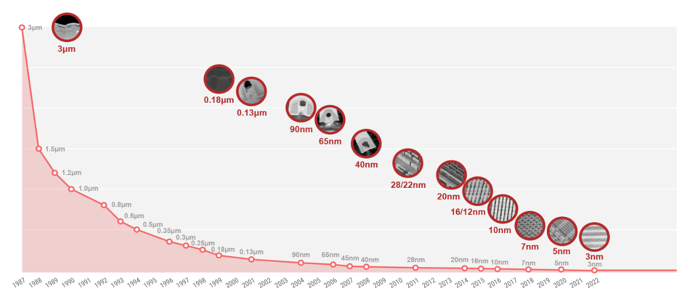
TSMC’s 5nm and 3nm Chips:
- Taiwan Semiconductor Manufacturing Company (TSMC) has been at the forefront of adopting EUVL. Their 5nm process node, which utilizes EUV lithography extensively, powers some of the latest high-performance chips. TSMC has also progressed to the 3nm node, promising further enhancements in power efficiency, performance, and transistor density.
Samsung’s 5nm and 3nm Chips:
- Samsung Foundry is another leading player in EUV technology. Their 5nm EUV process is used in a variety of applications, from mobile processors to high-performance computing chips. Samsung is also advancing to the 3nm node, which leverages EUV to push the boundaries of semiconductor performance.
Intel’s Alder Lake and Sapphire Rapids:
- Intel has integrated EUVL into its manufacturing processes with its Alder Lake processors, which are built on the Intel 7 (previously known as 10nm Enhanced SuperFin) and incorporate EUV at certain critical layers. Intel’s upcoming Sapphire Rapids processors, expected to utilize advanced EUV techniques, aim to enhance performance and power efficiency for data centers and enterprise applications.
Apple’s A15 and M1 Chips:
- Apple’s custom silicon, including the A15 Bionic chip and the M1 series for Macs, are manufactured using TSMC’s 5nm EUV process. These chips provide significant performance improvements and energy efficiency, powering the latest iPhones, iPads, and Mac computers.
Products Using EUV-Manufactured Chips
Smartphones:
- Apple iPhone 13 Series: Powered by the A15 Bionic chip, the iPhone 13 series benefits from the enhanced performance and energy efficiency provided by TSMC’s 5nm EUV process. This translates to faster processing speeds, better graphics performance, and improved battery life.
- Samsung Galaxy S21 Ultra: Featuring Samsung’s Exynos 2100 or Qualcomm’s Snapdragon 888 (both made using 5nm EUV technology), the Galaxy S21 Ultra offers top-tier performance, exceptional camera capabilities, and efficient power management.
Laptops and Tablets:
- Apple MacBook Air and MacBook Pro (M1): The M1 chip, manufactured using TSMC’s 5nm EUV process, delivers remarkable performance and battery life. It integrates CPU, GPU, and machine learning capabilities, setting new standards for portable computing.
- Microsoft Surface Pro X: Equipped with the Microsoft SQ2 processor, developed in partnership with Qualcomm and based on 5nm EUV technology, the Surface Pro X provides a balance of performance and battery efficiency for a versatile computing experience.
High-Performance Computing:
- NVIDIA GeForce RTX 30 Series: Utilizing Samsung’s 8nm process with EUV technology, the RTX 30 series GPUs offer unparalleled graphics performance, making them ideal for gaming, AI, and data-intensive applications.

- AMD Ryzen 5000 Series: Built on TSMC’s 7nm and utilizing some EUV layers, the Ryzen 5000 series processors deliver leading performance for desktops and laptops, catering to both gamers and professionals.
Data Centers and Enterprise Solutions:
- Intel Xeon Scalable Processors: The upcoming Sapphire Rapids processors, expected to leverage advanced EUV technology, aim to deliver significant improvements in performance and efficiency for data centers and enterprise applications.
- Amazon Web Services (AWS) Graviton2: Utilizing 7nm technology with EUV, AWS’s Graviton2 processors offer enhanced performance and cost-efficiency for cloud computing services, powering a wide range of AWS workloads.
Advantages of Latest Chips Made from EUVL Compared to Chips Made from Older Technology
The transition to Extreme Ultraviolet Lithography (EUVL) in semiconductor manufacturing has brought about significant improvements in chip performance and efficiency. One of the critical aspects that often gets discussed is the cost advantages of chips made using EUVL compared to those made using older lithographic technologies. Here’s an in-depth look at the various cost advantages associated with EUV-manufactured chips:
1. Enhanced Performance and Efficiency
Higher Transistor Density:
- EUVL enables the creation of smaller and more densely packed transistors. This higher transistor density leads to enhanced performance and power efficiency, allowing manufacturers to produce chips that deliver more computing power per unit area. This means fewer chips are needed to achieve the same performance, reducing the overall cost of deploying technology in devices.
Energy Savings:
- Chips made using EUVL are more energy-efficient. For data centers and enterprise applications, this translates into significant cost savings in terms of power consumption and cooling requirements. Lower energy consumption also extends battery life in mobile devices, adding value for consumers and reducing operational costs for manufacturers.
2. Simplified Manufacturing Process
Reduction in Multiple Patterning Steps:
- Older lithographic techniques, especially at nodes below 20nm, often require multiple patterning steps to achieve the desired resolution. These additional steps increase the complexity, time, and cost of manufacturing. EUVL, with its 13.5 nm wavelength, reduces or eliminates the need for multiple patterning, simplifying the process and lowering costs.
Yield Improvements:
- The precision of EUVL results in higher yield rates, meaning a higher percentage of wafers produced are usable and meet quality standards. Higher yields reduce the cost per functional chip, making the manufacturing process more economical.
3. Scalability and Future-Proofing
Long-Term Cost Reduction:
- While the initial setup and equipment costs for EUVL are high, the technology provides a scalable solution for future nodes. As the industry moves towards 3nm and beyond, EUVL offers a path to continue scaling down transistor sizes without exponentially increasing manufacturing costs. This future-proofing aspect provides long-term cost advantages as it avoids the need for frequent overhauls of manufacturing infrastructure.
Process Optimization:
- Continuous improvements in EUVL technology and processes lead to more efficient use of materials and resources. For instance, advancements in photoresist materials and pellicles enhance process reliability and reduce waste, further driving down costs over time.
4. Market Competitiveness and Product Value
Competitive Advantage:
- Manufacturers using EUVL can produce higher-performance chips at a lower cost, providing a competitive advantage in the market. This advantage allows them to offer better products at competitive prices, increasing market share and profitability.
Increased Product Lifespan:
- EUV-manufactured chips tend to have better performance characteristics, which can extend the lifespan of electronic devices. Consumers benefit from more durable and longer-lasting products, enhancing brand reputation and reducing the frequency of replacements, which indirectly lowers costs for both consumers and manufacturers.
5. Technological Innovations and Ecosystem Benefits
Collaborative Cost Sharing:
- The semiconductor industry’s collaborative approach to advancing EUVL technology, involving partnerships among manufacturers, equipment suppliers, and research institutions, helps share the high initial costs. These collaborations lead to shared innovations, spreading the benefits and reducing the financial burden on individual companies.
Economies of Scale:
- As more manufacturers adopt EUVL, economies of scale come into play. The increased demand for EUV equipment and materials drives down unit costs, making the technology more affordable and accessible. This scaling effect reduces costs across the industry, benefiting all stakeholders.
Also, Read: Unveiling Supercapacitors: Revolutionizing Energy Storage
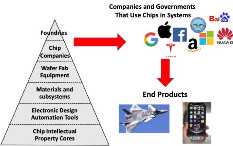
Primary companies with EUVL manufacturing capacity
Currently, several leading semiconductor companies have developed EUVL manufacturing capabilities. These companies are at the forefront of semiconductor innovation, leveraging EUVL to produce advanced chips.
Here are the primary companies with EUVL manufacturing capacity:
1. Taiwan Semiconductor Manufacturing Company (TSMC)
- Overview: TSMC is the world’s largest contract chipmaker and a pioneer in adopting EUVL for mass production.
- Technology Nodes: TSMC utilizes EUVL in its 5nm process node and is advancing towards 3nm and beyond.
- Products: TSMC manufactures chips for major clients like Apple (A15 and M1 chips), AMD (Ryzen processors), and NVIDIA (GeForce RTX GPUs).
2. Samsung Foundry
- Overview: Samsung Foundry is a major player in semiconductor manufacturing, investing heavily in EUVL.
- Technology Nodes: Samsung uses EUVL for its 5nm and upcoming 3nm process nodes.
- Products: Samsung produces chips for its own products, such as Exynos processors, as well as for external clients like Qualcomm (Snapdragon processors).
3. Intel Corporation
- Overview: Intel has been integrating EUVL into its manufacturing processes to maintain its competitiveness in advanced semiconductor technologies.
- Technology Nodes: Intel has incorporated EUVL in its Intel 7 process (previously 10nm Enhanced SuperFin) and is progressing towards using EUVL in more advanced nodes like Intel 4 (7nm EUV).
- Products: Intel’s EUV-based products include the Alder Lake processors and upcoming Sapphire Rapids processors for data centers and high-performance computing.
4. GlobalFoundries
- Overview: GlobalFoundries, while not as advanced in EUVL adoption as TSMC or Samsung, has been exploring EUVL for future nodes to stay competitive in the semiconductor market.
- Technology Nodes: The company is focusing on the development and potential integration of EUVL in its future process technologies.
Geopolitical Implications of EUVL
EUVL technology plays a significant role in the global semiconductor supply chain, and its strategic importance has geopolitical implications. The advanced capabilities provided by EUVL are crucial for producing the most sophisticated and high-performance chips, which are essential for various technological applications, from consumer electronics to defense systems.
1. Supply Chain Control
- Strategic Importance: EUVL technology is a key asset for maintaining a competitive edge in the semiconductor industry. Countries that possess this technology have significant leverage in the global tech ecosystem.
- Geopolitical Influence: The ability to produce advanced chips using EUVL technology can affect geopolitical dynamics, as countries and companies strive to secure access to the most advanced manufacturing capabilities. This can lead to strategic alliances and influence global supply chains.
2. Export Controls and Restrictions
- Regulatory Measures: Countries with leading EUVL capabilities, particularly the United States, have imposed export controls and restrictions to prevent the technology from being accessed by potential geopolitical adversaries. These measures aim to maintain technological superiority and national security.
- Impact on Trade: Export restrictions on EUVL equipment and technology can impact global trade relationships and semiconductor supply chains, potentially leading to geopolitical tensions.
3. Strategic Alliances and Investments
- Collaborations: Companies with EUVL capabilities often engage in strategic collaborations and investments to bolster their technology and market position. These partnerships can cross national borders and involve substantial investments in R&D and manufacturing infrastructure.
- Government Support: Governments may support their domestic semiconductor industries through subsidies, tax incentives, and funding for R&D to enhance their global competitiveness in EUVL technology.
4. Technological Sovereignty
- National Security: The ability to independently produce advanced semiconductors using EUVL is considered a matter of national security for many countries. Ensuring a secure and resilient semiconductor supply chain is critical for defense, communications, and critical infrastructure.
- Diversification Efforts: Countries are making efforts to diversify their semiconductor supply chains to reduce dependency on a few key players. This includes investing in domestic manufacturing capabilities and fostering innovation in alternative technologies.
Also, Read: Gamechanger: Sodium-ion batteries may make EVs far more affordable
Size Reduction in Products Using Chips Made from EUVL
The use of Extreme Ultraviolet Lithography (EUVL) in semiconductor manufacturing significantly impacts the size and performance of the resulting microchips. The primary advantage of EUVL is its ability to create much smaller and more densely packed transistors compared to older lithographic techniques. This miniaturization leads to substantial size reductions in the end products that use these chips. Here’s an overview of how EUVL contributes to the size reduction and overall benefits in various products:
1. Smaller Transistors and Higher Density
Feature Size Reduction:
- EUVL allows for the production of transistors with feature sizes as small as 5nm and even progressing towards 3nm. This is a considerable reduction compared to older technologies, such as Deep Ultraviolet (DUV) lithography, which is typically used for 10nm and larger nodes.
Increased Transistor Density:
- With smaller transistors, more of them can fit into a given area of a chip. This increased density enhances the chip’s computing power and efficiency without increasing its physical size.
2. Impact on End Product Sizes
Smartphones:
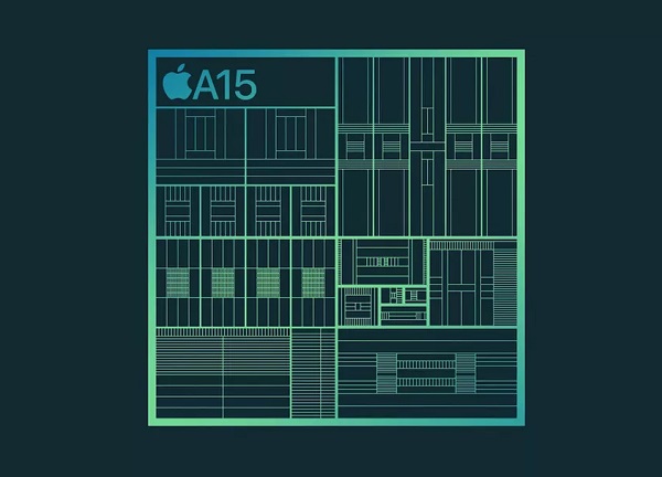
- Example: Apple’s iPhone 13 series uses the A15 Bionic chip, manufactured using TSMC’s 5nm EUV process.
- Size Reduction Impact: The A15 Bionic chip’s smaller transistors and increased efficiency allow for a more compact design of the phone’s logic board. This contributes to the overall slimness and light weight of modern smartphones, while also providing space for larger batteries and more advanced components like cameras and sensors.
Laptops and Tablets:
- Example: Apple’s MacBook Air and MacBook Pro with M1 chips, also made with TSMC’s 5nm EUV process.
- Size Reduction Impact: The M1 chip integrates multiple functions (CPU, GPU, RAM) into a single compact package. This integration reduces the motherboard size, enabling thinner and lighter laptop designs without sacrificing performance. Additionally, this allows for better thermal management and extended battery life.
Wearable Devices:
- Example: Samsung Galaxy Watch series using chips made from 5nm EUV technology.
- Size Reduction Impact: EUV-manufactured chips allow for more compact and power-efficient processors in wearable devices, contributing to slimmer, lighter designs with enhanced functionality and longer battery life.
3. Performance and Efficiency Gains
Enhanced Performance:
- Smaller transistors provide faster switching speeds and lower power consumption. This results in significant performance improvements in computing and processing tasks, enabling more powerful and feature-rich devices within the same physical dimensions.
Energy Efficiency:
- The energy efficiency of EUV-manufactured chips reduces the heat generated during operation. This efficiency allows for smaller cooling systems and contributes to the overall reduction in device size and weight.
4. Innovative Product Designs
Flexible and Foldable Electronics:
- The compact nature of EUV-manufactured chips enables innovative designs like foldable smartphones and flexible displays. These designs are possible because the internal components, including the logic boards and processors, occupy less space, allowing for more versatile form factors.
Compact IoT Devices:
- Internet of Things (IoT) devices benefit from the miniaturization enabled by EUVL. Smaller and more efficient chips allow for compact sensors, wearables, and other connected devices that can be discreetly integrated into various environments and applications.
Current Market Size and Growth in EUVL
The Extreme Ultraviolet Lithography (EUVL) market is experiencing significant growth, driven by the increasing demand for advanced semiconductor devices and the ongoing miniaturization of electronic components. The market size and growth projections for EUVL can be understood by examining the following key aspects:
1. Current Market Size
Market Valuation:
- As of 2023, the global EUVL market was valued at approximately USD 6.5 billion. This valuation includes the revenue generated from the sale of EUVL equipment, materials, and related services.
Major Players:
- The market is dominated by a few key players, with ASML being the leading manufacturer of EUV lithography machines. Other significant contributors include companies involved in producing EUV-specific materials and components, such as photomasks and photoresists.
2. Market Growth Projections
CAGR (Compound Annual Growth Rate):
- The EUVL market is projected to grow at a compound annual growth rate (CAGR) of around 15-20% from 2023 to 2030. This robust growth is fueled by the increasing adoption of EUV technology in semiconductor manufacturing, especially for advanced nodes like 7nm, 5nm, and 3nm.
Future Valuation:
- By 2030, the EUVL market is expected to exceed USD 15 billion, driven by continued investments in semiconductor fabrication facilities (fabs) and the expansion of EUV production capabilities.
3. Driving Factors for Growth
Technological Advancements:
- Continuous improvements in EUV technology, such as higher power light sources, more efficient photomasks, and better resist materials, are making EUVL more viable and cost-effective for mass production. These advancements are essential for maintaining the momentum of Moore’s Law.
Increasing Demand for Advanced Chips:
- The demand for smaller, more powerful, and energy-efficient chips is rising across various industries, including consumer electronics, automotive, telecommunications, and data centers. EUVL enables the production of these advanced chips, driving its adoption and market growth.
Expansion of Semiconductor Manufacturing:
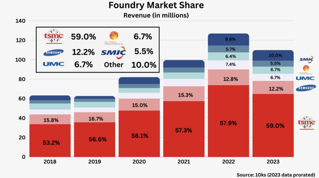
- Major semiconductor manufacturers like TSMC, Samsung, and Intel are heavily investing in expanding their EUV production capabilities. These investments are critical for scaling up the production of advanced nodes and meeting the global demand for cutting-edge semiconductors.
Government and Industry Initiatives:
- Governments and industry consortia are providing significant support for the development and deployment of EUV technology. Initiatives to strengthen semiconductor supply chains and ensure technological leadership are contributing to the growth of the EUVL market.
4. Regional Insights
Asia-Pacific:
- The Asia-Pacific region, particularly Taiwan, South Korea, and China, is leading the adoption of EUV technology. This region hosts major semiconductor fabs and accounts for the largest share of the EUVL market.
North America:
- The United States is a significant player in the EUVL market, with companies like Intel investing heavily in EUV technology. Additionally, government initiatives to bolster domestic semiconductor manufacturing are expected to drive further growth.
Europe:
- Europe, home to ASML, plays a crucial role in the EUVL market. The region benefits from being a hub for advanced lithography equipment manufacturing and innovation.
5. Challenges and Opportunities
High Costs and Technical Challenges:
- The high cost of EUV equipment and the technical challenges associated with EUV lithography, such as generating a stable light source and producing defect-free masks, remain significant hurdles. However, ongoing research and development efforts are addressing these challenges, opening up new opportunities for market growth.
Emerging Applications:
- Emerging applications in artificial intelligence (AI), 5G, autonomous vehicles, and the Internet of Things (IoT) are creating new demand for advanced semiconductor devices. EUVL is crucial for producing the high-performance chips needed for these applications, presenting further growth opportunities.
The EUVL market is poised for substantial growth, driven by technological advancements, increasing demand for advanced semiconductor devices, and significant investments in manufacturing capabilities. With a projected CAGR of 15-20% over the next decade, the market is expected to exceed USD 15 billion by 2030. As the industry continues to overcome technical challenges and expand its adoption of EUV technology, the EUVL market will play a critical role in shaping the future of semiconductor manufacturing.
High NA (Numerical Aperture) EUV Lithography
High Numerical Aperture (NA) EUV Lithography represents a significant advancement in Extreme Ultraviolet Lithography (EUVL) technology. It is designed to further enhance the resolution and patterning capabilities of EUV systems, enabling the production of even smaller and more complex semiconductor devices. Here’s a detailed look at what High NA EUV Lithography is, its benefits, and its impact on the semiconductor industry.
1. Understanding Numerical Aperture (NA)
Numerical Aperture (NA) Definition:
- NA is a dimensionless number that characterizes the range of angles over which a system can accept or emit light. In the context of lithography, it describes the ability of the optics to focus light onto the wafer.
High NA vs. Conventional NA:
- Conventional EUV systems typically have a NA of 0.33. High NA EUV systems increase this value to 0.55, allowing for improved resolution and depth of focus.
2. Technical Advancements in High NA EUV Lithography
Optical System Enhancements:
- High NA EUV lithography involves redesigning the optical system of the EUV scanner. This includes using larger and more precisely engineered mirrors to accommodate the increased NA.
Shorter Wavelength Utilization:
- While standard EUV uses a 13.5 nm wavelength, High NA systems can more effectively utilize this wavelength due to the improved focusing capability provided by the higher NA.
Pellicle and Mask Innovations:
- High NA systems require advancements in mask and pellicle technology to handle the increased resolution and precision demands. This includes the development of new materials and designs that can maintain performance under higher NA conditions.
3. Benefits of High NA EUV Lithography
Enhanced Resolution:
- The primary benefit of High NA EUV is its ability to produce finer feature sizes on semiconductor wafers. With higher NA, the system can resolve smaller details, pushing the limits of Moore’s Law further.
Increased Patterning Accuracy:
- Higher NA improves the depth of focus, which enhances patterning accuracy and reduces defects. This is crucial for producing high-quality, reliable semiconductor devices.
Greater Design Flexibility:
- The improved resolution and accuracy allow for more complex and densely packed circuit designs, enabling the development of more powerful and efficient chips.
4. Impact on Semiconductor Manufacturing
Next-Generation Nodes:
- High NA EUV lithography is critical for manufacturing nodes beyond 3nm. It provides the necessary capabilities to continue scaling down feature sizes, essential for future generations of microprocessors and memory chips.
Advanced Applications:
- The technology supports the development of advanced applications in artificial intelligence (AI), 5G, autonomous vehicles, and the Internet of Things (IoT). These applications require chips with higher performance and efficiency, which High NA EUV can deliver.
Economic and Competitive Advantage:
- Semiconductor manufacturers that adopt High NA EUV lithography gain a significant competitive edge by being able to produce more advanced and efficient chips. This can lead to economic benefits and market leadership in the semiconductor industry.
5. Challenges and Development
Technical Challenges:
- Implementing High NA EUV lithography presents several technical challenges, including the development of new optical components, masks, and pellicles that can operate effectively at higher NA.
Cost Considerations:
- The transition to High NA EUV involves substantial investment in new equipment and infrastructure. This includes the cost of developing and manufacturing new optical systems and the associated R&D expenses.
Industry Collaboration:
- Overcoming these challenges requires collaboration among semiconductor manufacturers, equipment suppliers, and research institutions. Joint efforts and shared innovations are crucial for the successful deployment of High NA EUV technology.

6. Future Outlook
Deployment Timeline:
- High NA EUV lithography is expected to be deployed in the mid-2020s, with leading companies like ASML developing the necessary equipment. The industry is closely watching these developments to prepare for the integration of High NA systems into semiconductor fabs.
Long-Term Benefits:
- In the long term, High NA EUV lithography will play a vital role in sustaining the pace of semiconductor innovation. It will enable the production of chips that meet the ever-increasing demands for performance, efficiency, and miniaturization in modern technology.
High NA EUV Lithography represents a crucial advancement in semiconductor manufacturing technology, providing the means to further scale down feature sizes and improve chip performance. By increasing the Numerical Aperture of EUV systems, this technology enhances resolution and patterning accuracy, enabling the production of next-generation semiconductor devices. While it presents technical and economic challenges, the collaborative efforts within the industry and the significant potential benefits make High NA EUV lithography a pivotal development for the future of the semiconductor industry.
Patterning Using Multi-Trigger Resist
Patterning using multi-trigger resist is an advanced technique in the field of semiconductor lithography, particularly relevant to Extreme Ultraviolet Lithography (EUVL). This method aims to improve the resolution, sensitivity, and line-edge roughness (LER) of the photoresist used in the lithography process. Here’s a detailed look at what multi-trigger resist is, how it works, and its benefits in semiconductor manufacturing.
1. Understanding Multi-Trigger Resist
Photoresist Basics:
- A photoresist is a light-sensitive material applied to a substrate (usually a silicon wafer) that undergoes chemical changes when exposed to light. These changes allow for the selective removal of either the exposed or unexposed regions, creating a pattern on the substrate.
Multi-Trigger Resist Concept:
- Traditional photoresists rely on a single exposure event to initiate the chemical changes required for pattern development. Multi-trigger resists, on the other hand, are designed to respond to multiple exposure triggers. These triggers can be various wavelengths of light, different intensities, or a combination of exposure and chemical amplification processes.
2. Mechanism of Multi-Trigger Resist
Multiple Exposure Events:
- Multi-trigger resists utilize more than one exposure event to achieve the desired chemical transformation. For example, the resist may require exposure to EUV light followed by a secondary exposure to a different wavelength or an additional chemical treatment to fully activate the resist’s patterning properties.
Chemical Amplification:
- These resists often incorporate chemical amplification mechanisms where a single photon event triggers a cascade of chemical reactions, amplifying the initial exposure. This approach increases the sensitivity of the resist, allowing for lower doses of EUV light to achieve the necessary patterning.
Dual-Tone and Multi-Tone Patterning:
- Multi-trigger resists can be designed to exhibit dual-tone (positive and negative tone) or multi-tone behavior, depending on the exposure and processing conditions. This flexibility allows for more complex and precise patterning capabilities.
3. Benefits of Multi-Trigger Resist
Enhanced Resolution:
- By requiring multiple triggers to fully develop the pattern, multi-trigger resists can achieve higher resolution than single-trigger resists. The finer control over the chemical reactions allows for sharper and more defined features on the wafer.
Improved Sensitivity:
- The chemical amplification process inherent in multi-trigger resists significantly enhances their sensitivity. This means that lower doses of EUV light are required, which can reduce the overall exposure time and improve throughput in the lithography process.
Reduced Line-Edge Roughness (LER):
- Line-edge roughness refers to the variability in the edge of a patterned line. Multi-trigger resists can reduce LER by providing a more controlled and uniform reaction across the exposed regions, resulting in smoother and more precise edges.
Greater Process Latitude:
- Multi-trigger resists offer greater flexibility in processing conditions. The ability to use different exposure wavelengths or additional chemical treatments allows for more robust patterning processes that can be fine-tuned to meet specific manufacturing requirements.
4. Applications in Semiconductor Manufacturing
Advanced Node Fabrication:
- Multi-trigger resists are particularly useful for fabricating advanced semiconductor nodes (e.g., 7nm, 5nm, and below). The enhanced resolution and sensitivity are critical for producing the extremely small and densely packed features required at these technology nodes.
Complex Device Architectures:
- The flexibility of multi-trigger resists makes them suitable for patterning complex device architectures, such as 3D NAND, FinFETs, and other advanced semiconductor structures. The precise control over feature dimensions and placement is crucial for these applications.
EUV Lithography Enhancement:
- As EUVL pushes the boundaries of traditional lithography, multi-trigger resists provide the necessary improvements in resist performance to fully leverage the capabilities of EUV light. They help address some of the current limitations in EUV patterning, such as resolution, sensitivity, and LER.
5. Challenges and Development
Complexity and Cost:
- The development and implementation of multi-trigger resists are more complex than traditional resists. This complexity can lead to higher costs in both development and manufacturing. However, the benefits in performance and efficiency can outweigh these costs in high-volume production environments.
Process Integration:
- Integrating multi-trigger resists into existing lithography workflows requires careful consideration of the entire process, from exposure to development. Ensuring compatibility with current equipment and optimizing processing parameters are critical for successful adoption.
Research and Collaboration:
- Ongoing research and collaboration among semiconductor manufacturers, material scientists, and equipment suppliers are essential for advancing multi-trigger resist technology. These efforts focus on improving resist formulations, understanding the underlying mechanisms, and optimizing process integration.
Patterning using multi-trigger resist is a promising advancement in semiconductor lithography, particularly for EUV applications. By leveraging multiple exposure triggers and chemical amplification, multi-trigger resists offer significant improvements in resolution, sensitivity, and line-edge roughness. These benefits make them ideal for advanced node fabrication and complex device architectures. While there are challenges in development and integration, the potential advantages of multi-trigger resists make them a crucial technology for the future of semiconductor manufacturing.
Carbon Nanotube EUV Pellicles
As Extreme Ultraviolet Lithography (EUVL) becomes increasingly essential for advanced semiconductor manufacturing, the need for reliable pellicles has become more critical. Pellicles are thin membranes placed over photomasks to protect them from contamination during the lithography process. The development of carbon nanotube (CNT) EUV pellicles represents a significant advancement in this area, offering enhanced performance and durability. Here’s a detailed look at carbon nanotube EUV pellicles, their advantages, and their impact on semiconductor manufacturing.
1. What are Carbon Nanotube EUV Pellicles?
Carbon Nanotubes (CNTs):
- Carbon nanotubes are cylindrical nanostructures composed of carbon atoms arranged in a hexagonal lattice. They possess extraordinary mechanical, electrical, and thermal properties, making them ideal for various advanced applications.
EUV Pellicles:
- In EUVL, pellicles are used to protect photomasks from particle contamination. Given the short wavelength (13.5 nm) and high energy of EUV light, traditional pellicle materials often fail to provide the necessary transparency and durability. CNTs offer a promising solution due to their unique properties.
2. Properties of Carbon Nanotube Pellicles
High Transparency:
- CNT pellicles exhibit high transparency to EUV light, allowing more than 90% of the light to pass through. This high transparency is crucial for maintaining the intensity of the EUV light reaching the wafer, ensuring effective pattern transfer.
Mechanical Strength:
- CNTs are incredibly strong and flexible, providing robust mechanical protection to the photomask. Their high tensile strength ensures that the pellicle can withstand the rigors of the lithography process without deforming or breaking.
Thermal Stability:
- CNT pellicles can endure the high temperatures generated during EUV exposure. Their excellent thermal conductivity helps dissipate heat, preventing damage to the pellicle and the underlying photomask.
Chemical Resistance:
- The chemical stability of CNTs makes them resistant to various processing chemicals used in semiconductor manufacturing. This resistance ensures the longevity and reliability of the pellicle throughout the lithographic process.
3. Advantages of Carbon Nanotube EUV Pellicles
Enhanced Protection:
- CNT pellicles provide superior protection for photomasks by preventing particle contamination. This protection is essential for maintaining the integrity of the photomask and ensuring high-quality pattern transfer.
Improved Yield and Throughput:
- By reducing defects caused by contamination, CNT pellicles improve the yield of functional chips. Higher yields translate to lower manufacturing costs and increased throughput, making the overall process more efficient.
Longevity and Durability:
- The robustness and durability of CNT pellicles mean they have a longer operational life compared to traditional pellicles. This longevity reduces the frequency of pellicle replacements, lowering maintenance costs and downtime.
Scalability for Advanced Nodes:
- As semiconductor nodes continue to shrink, the demands on pellicle performance increase. CNT pellicles are scalable to advanced nodes (e.g., 7nm, 5nm, and beyond), supporting the production of smaller, more complex semiconductor devices.
4. Challenges in Developing CNT EUV Pellicles
Manufacturing Complexity:
- Producing high-quality CNT pellicles involves sophisticated manufacturing techniques. Ensuring uniformity and consistency in CNT arrangement and alignment is challenging and requires advanced fabrication methods.
Integration with Existing Processes:
- Integrating CNT pellicles into existing EUVL workflows necessitates modifications to lithography equipment and processes. Ensuring compatibility and optimizing these processes are critical for successful adoption.
Cost Considerations:
- The initial development and production costs of CNT pellicles are higher compared to traditional materials. However, the long-term benefits in terms of performance, durability, and yield can justify these costs.
5. Impact on Semiconductor Manufacturing
Advanced Node Production:
- CNT EUV pellicles enable the production of advanced semiconductor nodes with higher precision and reliability. Their use supports the ongoing miniaturization of semiconductor devices, essential for modern electronics.
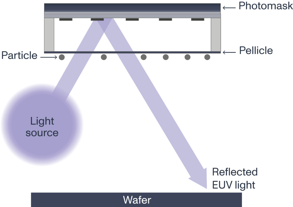
Increased Efficiency and Lower Defect Rates:
- By providing superior protection and reducing defect rates, CNT pellicles contribute to more efficient manufacturing processes. This efficiency helps semiconductor manufacturers meet the high demand for advanced chips while maintaining quality.
Support for Emerging Technologies:
- The enhanced performance of CNT pellicles is crucial for supporting emerging technologies such as artificial intelligence (AI), 5G, and the Internet of Things (IoT). These technologies require high-performance chips that can be reliably produced using advanced lithography techniques.
DNP Develops Photomask Process for 3nm EUV Lithography
Dai Nippon Printing Co., Ltd. (DNP) has achieved a significant milestone in semiconductor manufacturing with the development of a new photomask manufacturing process tailored for 3-nanometer (nm) Extreme Ultraviolet (EUV) lithography. This advancement is poised to meet the semiconductor industry’s escalating demand for increasingly finer circuit line widths, crucial for the production of next-generation microchips.
Background and History
DNP has a notable history of innovation in photomask technology:
- Pioneering Multi-Beam Mask Writing Tool (MBMW): In 2016, DNP became the first merchant photomask manufacturer to introduce the MBMW, a tool that has revolutionized the precision and efficiency of photomask production.
- 5nm EUV Lithography: In 2020, DNP developed a photomask process for 5nm EUV lithography, setting a new standard in the industry and paving the way for advanced semiconductor devices.
New Photomask Process for 3nm EUV Lithography
The newly developed process by DNP incorporates several cutting-edge manufacturing techniques and data correction technologies designed to handle the complexity of 3nm nodes:
- Enhanced Manufacturing Techniques: The new process utilizes advanced fabrication methods to achieve the precise patterning required for 3nm circuits. These techniques ensure the accuracy and reliability of the photomasks, which are critical for successful EUV lithography.
- Data Correction Technology: Improved data correction algorithms support the creation of complex curved pattern structures that are essential for EUV lithography at such fine scales. This technology compensates for potential distortions and ensures the fidelity of the photomask patterns.
Future Plans and Market Impact
Operational Timeline:
- DNP plans to commence operations with a new Multi-Beam Mask Writing Tool (MBMW) in the second half of 2024. This new equipment will enhance their capacity to produce high-precision photomasks for 3nm EUV lithography.
Sales Projections:
- By 2030, DNP aims to achieve annual sales of 10 billion yen through the production and sale of these advanced photomasks. This projection reflects the growing demand for smaller, more powerful semiconductor devices across various industries.
Market Significance:
- The development of a 3nm photomask process underscores DNP’s commitment to leading the industry in photomask technology. It addresses the critical need for precision and reliability in semiconductor manufacturing as the industry continues to push the boundaries of miniaturization.
EUV Machine Manufacturers
1. ASML Holding N.V.
Overview:
- ASML, a Dutch company, is the world leader in the production of EUV lithography machines. It is the only company that currently offers EUV machines capable of high-volume manufacturing.
Products:
- ASML’s EUV lithography systems, such as the Twinscan NXE series, are used by major semiconductor manufacturers to produce chips at advanced nodes like 7nm, 5nm, and 3nm.
Technology:
- ASML’s EUV machines utilize a highly complex system that includes a laser-produced plasma (LPP) light source, advanced optics, and precision engineering to achieve the desired resolution and patterning capabilities. The company has continually improved its systems to enhance performance, throughput, and reliability.
Customers:
- Major customers of ASML include leading semiconductor manufacturers such as TSMC, Samsung, and Intel, who use ASML’s EUV machines to produce advanced semiconductor devices.
2. Carl Zeiss SMT
Role:
- Carl Zeiss SMT, a subsidiary of the German optics company Carl Zeiss AG, plays a crucial role in the EUV ecosystem by providing the critical optical components used in ASML’s EUV lithography machines.
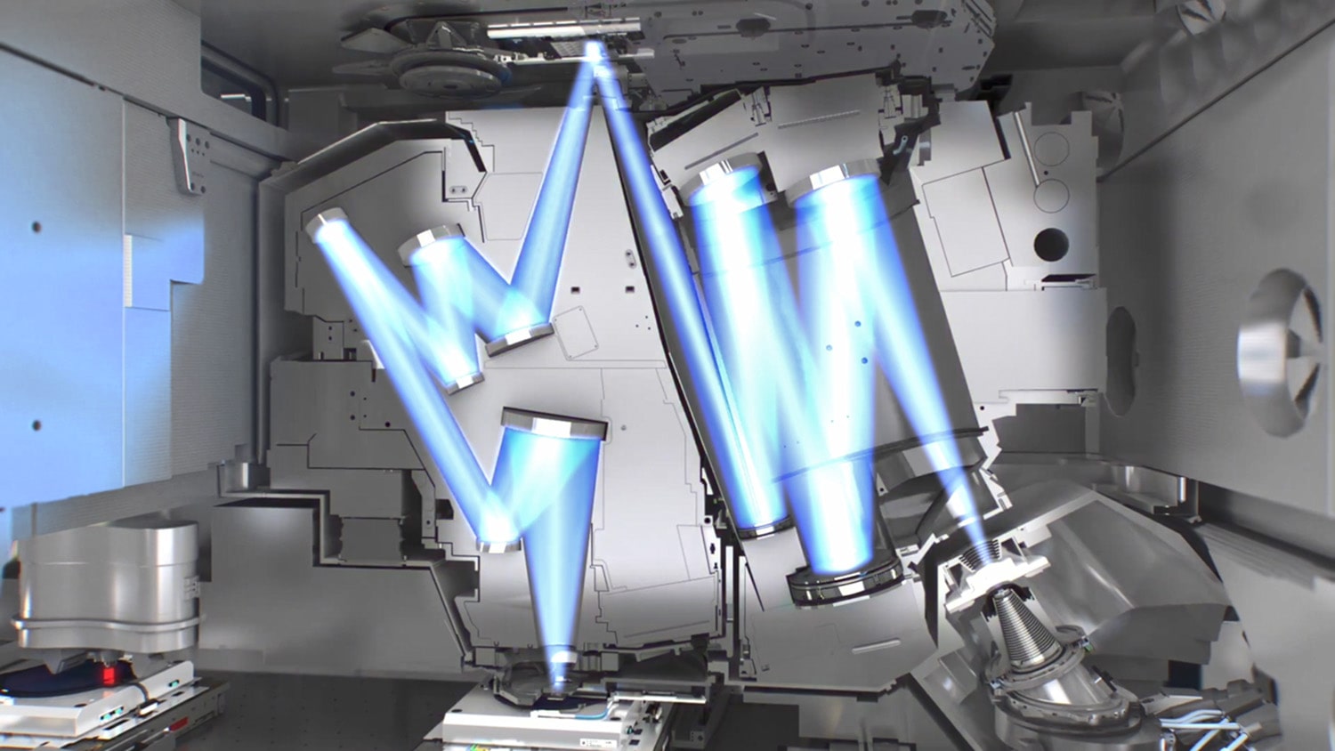
Products:
- Zeiss supplies the high-precision mirrors and lenses that are essential for the EUV lithography process. These optical components are designed to handle the unique challenges posed by EUV light, such as extreme precision and high reflectivity.
Collaboration with ASML:
- Carl Zeiss SMT collaborates closely with ASML to ensure that their optical systems meet the stringent requirements of EUV lithography. This partnership is vital for the successful deployment and operation of ASML’s EUV machines.
3. Gigaphoton Inc.
Overview:
- Gigaphoton, a Japanese company, is a notable supplier of light sources for lithography systems, including EUV light sources.
Products:
- The company develops and produces advanced laser-produced plasma (LPP) light sources, which are critical components of EUV lithography systems. These light sources generate the EUV light necessary for the lithography process by ionizing tin droplets with high-powered lasers.
Technological Contributions:
- Gigaphoton’s innovations in EUV light source technology contribute to improving the stability, power, and efficiency of EUV lithography machines.
The market for EUV lithography machines is highly specialized, with ASML Holding N.V. being the dominant player in producing complete EUV systems for high-volume semiconductor manufacturing. Carl Zeiss SMT provides the essential optical components, while companies like Gigaphoton contribute by supplying advanced light sources. These companies collectively enable the semiconductor industry to produce the next generation of advanced microchips, driving forward the capabilities of modern electronic devices.
How an EUV Machine is Made?
Building an Extreme Ultraviolet Lithography (EUV) machine is a highly complex and intricate process that involves numerous advanced technologies and precise engineering. The process requires the integration of multiple subsystems, each meticulously designed and manufactured. Here’s an overview of how an EUV machine is made:
1. Design and Engineering
Conceptual Design:
- The process starts with the conceptual design, where engineers and scientists define the specifications and requirements for the EUV machine. This includes the desired resolution, throughput, and compatibility with semiconductor manufacturing processes.
Detailed Engineering:
- Detailed engineering designs are developed, incorporating mechanical, optical, and electronic systems. Computer-aided design (CAD) software is used to create detailed blueprints and simulations to ensure all components will work together seamlessly.
2. Key Components and Subsystems
EUV Light Source:
- Laser-Produced Plasma (LPP): The EUV light source is typically generated using a laser-produced plasma (LPP) method. This involves a high-power laser that hits tiny tin droplets, creating a plasma that emits EUV light at a wavelength of 13.5 nm.
- Laser System: The laser system is one of the most critical components and requires precise engineering to generate the necessary energy levels. Companies like Gigaphoton and Cymer (a subsidiary of ASML) are leading suppliers of these high-powered laser systems.
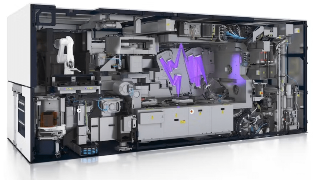
Multilayer Mirrors:
- Fabrication: Multilayer mirrors, composed of alternating layers of molybdenum (Mo) and silicon (Si), are fabricated to reflect the EUV light efficiently. These mirrors are produced with atomic-level precision using techniques like magnetron sputtering.
- Assembly: The mirrors are carefully assembled into the optical system of the EUV machine. Carl Zeiss SMT is a key supplier of these high-precision optical components.
Photomask (Reticle) Handling:
- Mask Production: Photomasks are produced using advanced lithographic techniques. They consist of a substrate (usually quartz) with an absorbing layer that defines the circuit patterns.
- Mask Handling System: The EUV machine includes a sophisticated system for loading, aligning, and handling the photomask with extreme precision.
Wafer Handling and Stage:
- Wafer Stage: The wafer stage moves the silicon wafer with nanometer precision under the EUV light. This stage must be incredibly stable and precise to ensure accurate patterning.
- Handling System: Automated systems are used to load and unload wafers, maintaining a vacuum environment to prevent contamination.
Vacuum and Environmental Control:
- Vacuum Chambers: EUV lithography requires a vacuum environment to prevent the EUV light from being absorbed by air. The machine includes multiple vacuum chambers with advanced pumping systems to maintain the required vacuum levels.
- Environmental Controls: Temperature and vibration control systems are integrated to ensure the stability and accuracy of the lithography process.
3. Assembly and Integration
Component Manufacturing:
- Each component and subsystem is manufactured to precise specifications. This includes machining, assembling, and testing individual parts.
Integration:
- The components are integrated into the main EUV machine. This step requires meticulous alignment and calibration to ensure all parts work together harmoniously. The integration process involves assembling the light source, optical systems, wafer stage, and control systems into a single unit.
Calibration and Testing:
- After assembly, the EUV machine undergoes extensive calibration and testing. This includes verifying the alignment of optical components, the performance of the laser system, and the accuracy of the wafer stage.
4. Software and Control Systems
Control Software:
- Advanced software is developed to control the EUV machine’s operations. This software manages the laser pulses, the movement of the wafer stage, the alignment of the photomask, and the overall coordination of the lithography process.
Real-Time Monitoring:
- Real-time monitoring systems are integrated to provide continuous feedback and adjustments. These systems ensure the machine operates within the specified parameters and can quickly respond to any deviations.
5. Final Testing and Quality Assurance
Performance Testing:
- The fully assembled EUV machine undergoes rigorous performance testing to ensure it meets all specifications. This includes testing for resolution, throughput, and repeatability.
Quality Assurance:
- Quality assurance processes are implemented to verify the reliability and durability of the machine. This includes stress testing under various conditions to ensure long-term performance.
6. Delivery and Installation
Transportation:
- Once the EUV machine passes all tests, it is carefully disassembled into transportable modules and shipped to the semiconductor manufacturer.
On-Site Installation:
- The machine is reassembled and installed at the customer’s site. This includes recalibrating and testing the machine to ensure it operates correctly in its new environment.
Training and Support:
- Comprehensive training is provided to the customer’s technical staff. Ongoing support and maintenance services are also established to ensure the machine’s optimal performance.
Size and Dimensions of an EUV Machine
Extreme Ultraviolet Lithography (EUV) machines are among the most complex and sophisticated pieces of equipment in semiconductor manufacturing. Their size and dimensions reflect the intricate technology and numerous subsystems required to generate, manipulate, and use EUV light for advanced lithography. Here is an overview of the typical size and dimensions of an EUV machine:
1. Overall Footprint
Footprint Dimensions:
- The overall footprint of an EUV machine is substantial, typically occupying an area of about 10 meters by 10 meters (approximately 100 square meters or 1,076 square feet). This space is necessary to accommodate all the components, including the light source, optical systems, wafer handling mechanisms, and environmental control units.
2. Height and Volume
Height:
- An EUV machine generally stands around 4 to 5 meters tall (approximately 13 to 16 feet). This height is needed to house the complex optical systems and maintain the necessary vacuum environment.
Volume:
- Considering its footprint and height, the total volume of an EUV machine is quite large, reflecting the extensive infrastructure and numerous subsystems required for its operation.
3. Key Components and Their Sizes
Light Source Module:
- Dimensions: The laser-produced plasma (LPP) light source module, including the laser system and tin droplet generator, is a significant component, often requiring a dedicated space of around 2 meters by 2 meters by 3 meters (approximately 6.5 feet by 6.5 feet by 10 feet).
- Function: This module generates the EUV light by ionizing tin droplets with high-powered laser pulses.
Optical Column:
- Dimensions: The optical column, containing the multilayer mirrors and reflective optics, typically extends vertically and can be around 2 meters in diameter and 3 to 4 meters in height (approximately 6.5 feet in diameter and 10 to 13 feet in height).
- Function: This column focuses and directs the EUV light onto the wafer with high precision.
Wafer Handling System:
- Dimensions: The wafer stage and handling system occupy a significant portion of the machine’s footprint, requiring an area of about 3 meters by 3 meters (approximately 10 feet by 10 feet).
- Function: This system moves the wafer with nanometer precision to ensure accurate patterning.
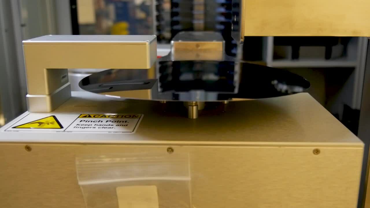
Vacuum Chambers:
- Dimensions: Multiple vacuum chambers are integrated throughout the machine, each varying in size. The largest chambers, housing the optical system and wafer stage, can be around 4 meters by 4 meters by 4 meters (approximately 13 feet by 13 feet by 13 feet).
- Function: These chambers maintain the vacuum environment necessary for EUV lithography to prevent absorption of EUV light by air.
Cooling and Environmental Control Systems:
- Dimensions: These auxiliary systems are essential for maintaining the operational stability of the EUV machine and typically require additional space around the main machine, often adding several meters to the overall footprint.
- Function: They manage the temperature, vibrations, and cleanliness of the environment within the EUV machine.
4. Installation Requirements
Cleanroom Environment:
- EUV machines are installed in cleanrooms with stringent cleanliness standards (typically Class 1 or better). The cleanroom area needs to be large enough to accommodate the machine and provide space for maintenance and operation, often extending the required footprint to around 200 square meters (approximately 2,152 square feet).
Infrastructure Support:
- The installation of an EUV machine requires robust infrastructure support, including power supplies, cooling systems, and vibration isolation. This infrastructure further increases the overall space requirements and complexity of the installation process.
- An EUV lithography machine is a massive and complex piece of equipment, typically occupying a footprint of around 100 square meters and standing 4 to 5 meters tall. Key components like the light source module, optical column, wafer handling system, and vacuum chambers each have substantial dimensions, contributing to the overall size of the machine. The installation of an EUV machine also demands a well-equipped cleanroom environment and extensive infrastructure support. This considerable size and complexity reflect the advanced technology and precision required to produce the next generation of semiconductor devices.
About Right Patents
Right Patents is a Reliable and Leading Patent Services Provider Company in the United States. We provide Top-Quality and Most Trusted Patent Drawing Services, Patentability Searches, Invalidity Searches, FTO Searches, and Patent Landscapes.
