The Future of Electronics – Diamond Semiconductors: Semiconductors are the foundation of modern electronics, critical to the functioning of a wide array of devices, including computers, smartphones, medical equipment, and renewable energy systems. Traditionally, semiconductor technology has relied heavily on materials like silicon and gallium nitride. Silicon, in particular, has been the dominant material due to its abundance, cost-effectiveness, and suitable electronic properties. However, the pursuit of materials that can offer better performance, higher efficiency, and greater robustness has led researchers to explore alternatives, with diamond emerging as a particularly promising candidate.
Diamond is renowned for its exceptional hardness, optical transparency, and thermal conductivity. These properties, along with its ability to operate at high voltages and temperatures, make diamond an attractive material for semiconductor applications. This article delves into the world of diamond semiconductors, exploring their unique properties, advantages, applications, current research, market potential, and real-world implementations. Also, Read: What are Tunnel Field-Effect Transistors (TFETs)?
What Are Diamond Semiconductors?
Diamond semiconductors refer to electronic devices that use diamond as the primary semiconductor material. The term “semiconductor” describes materials that have electrical conductivity between that of a conductor and an insulator. Semiconductors are crucial for the fabrication of electronic components like transistors, diodes, and integrated circuits.
Unique Properties of Diamond:
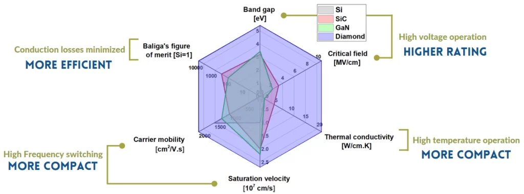
- Exceptional Thermal Conductivity: Diamond boasts a thermal conductivity of approximately 2200 W/m·K, which is significantly higher than other materials like silicon (around 150 W/m·K) and even metals like copper (approximately 400 W/m·K). This property enables diamond semiconductors to efficiently dissipate heat, which is critical for maintaining performance and reliability in high-power applications.
- High Breakdown Voltage: The breakdown voltage of a material is the voltage at which it becomes electrically conductive. Diamopnd’s high breakdown voltage allows it to handle high voltages without deteriorating, making it ideal for power electronics that require robust voltage handling capabilities.
- Wide Bandgap: Diamond has a wide bandgap of 5.5 eV compared to silicon’s 1.1 eV. A wide bandgap means that diamond can function effectively at higher temperatures and voltages. This property is crucial for applications in extreme environments where conventional semiconductors would fail.
- High Electron Mobility: Electron mobility is a measure of how quickly electrons can move through a material. Diamond’s high electron mobility allows for faster and more efficient electronic devices, particularly beneficial in high-frequency applications. Also, Read: Lithography in Semiconductor Manufacturing: Complete Guide
Advantages of Diamond Semiconductors
The unique properties of diamond semiconductors confer several significant advantages over traditional semiconductor materials like silicon and gallium nitride.
Thermal Management:
Diamond’s unparalleled thermal conductivity is one of its most significant advantages. Efficient heat dissipation is crucial in high-power electronic devices to prevent overheating, which can lead to performance degradation and device failure. Diamond’s ability to conduct heat away from active regions of a semiconductor device ensures stable operation and prolonged device lifespan, particularly in high-power and high-frequency applications.
Power Handling:
Diamond’s high breakdown voltage enables it to operate at much higher voltages and currents than silicon-based devices. This makes diamond semiconductors suitable for applications that require robust power handling capabilities. For instance, in power grids, diamond semiconductors can enhance efficiency and reliability, and in electric vehicles, they can improve performance and extend the range by handling higher power loads more efficiently.
Efficiency:
The high electron mobility of diamond allows for more efficient electronic performance, especially in high-frequency applications such as telecommunications and radar systems. Devices made from diamond can operate at higher speeds with lower energy loss, resulting in faster and more efficient signal processing and transmission.
Durability:
Diamond’s inherent hardness and resistance to radiation and chemical degradation make it an ideal material for use in harsh environments. This durability is particularly beneficial in aerospace and defense applications, where electronic components must withstand extreme conditions. Diamond’s robustness ensures long-term reliability and reduces the need for frequent replacements. Also, Read: What is Edge Computing? Complete Guide
Real-Life Products Using Diamond Semiconductors
The integration of diamond semiconductors into real-life products is still in its nascent stages, but several cutting-edge applications and products are leveraging the unique properties of diamond to push the boundaries of technology. Here are some notable examples:
High-Power Electronics
Power Grids and Electrical Infrastructure:
- Diamond-based Power Inverters: These inverters are used in power grids to convert direct current (DC) to alternating current (AC) with high efficiency and minimal energy loss. Companies like Element Six are developing diamond semiconductors to enhance the performance of power grid components.
Electric Vehicles (EVs):
- Power Control Units (PCUs): Diamond semiconductors are being explored for use in PCUs of electric vehicles to manage power flow more efficiently and extend battery life. Toyota is researching diamond-based PCUs to improve the performance and range of their EVs.
Telecommunications
High-Frequency Communication Devices:
- Microwave and RF Transistors: Diamond semiconductors are used in transistors for microwave and radio-frequency (RF) applications, which are critical in telecommunications and radar systems. These transistors offer higher power output and efficiency compared to traditional materials.
5G Technology:
- Diamond-based Amplifiers: In 5G networks, diamond semiconductors can be used in amplifiers to enhance signal strength and quality, supporting faster and more reliable communication. Researchers at the University of Bristol are working on diamond semiconductor amplifiers for 5G applications.
Medical Devices
Advanced Imaging Equipment:
- Diamond X-ray Detectors: Diamond semiconductors are used in X-ray detectors for medical imaging. These detectors provide high sensitivity and resolution, improving diagnostic capabilities. Companies like Diamcad are developing diamond-based X-ray detectors for medical applications.
Implantable Medical Devices:
- Biocompatible Electronics: Diamond’s biocompatibility makes it suitable for use in implantable medical devices, such as pacemakers and neurostimulators. These devices benefit from diamond’s durability and high performance.
Aerospace and Defense
Radiation-Hardened Electronics:
- Diamond-based Microchips: In aerospace and defense, diamond semiconductors are used in microchips that need to withstand high levels of radiation and extreme temperatures. These chips are critical for satellite systems and military communication devices.
High-Power Lasers:
- Diamond Lasers for Targeting and Communication: Diamond semiconductors are used in high-power laser systems for targeting and communication in defense applications. These lasers offer superior performance and reliability.
Consumer Electronics
High-Performance Computing:
- Diamond Heat Spreaders: In high-performance computing, diamond-based heat spreaders are used to manage heat dissipation in processors and graphics cards. These heat spreaders improve the performance and lifespan of computing devices.
Next-Generation LEDs:
- Diamond-based Light Emitting Diodes (LEDs): Diamond semiconductors are being explored for use in LEDs, offering higher brightness and efficiency. These LEDs can be used in advanced display technologies and lighting solutions.
Renewable Energy
Solar Inverters:
- Diamond-based Solar Inverters: In solar energy systems, diamond semiconductors are used in inverters to convert solar energy into usable electrical power with high efficiency. These inverters enhance the overall performance and reliability of solar power systems.
Wind Turbine Power Electronics:
- Power Converters: Diamond semiconductors are used in power converters for wind turbines, improving energy conversion efficiency and reliability.
Quantum Computing:
Diamond’s unique atomic structure and electron properties hold significant potential for quantum computing. Diamond can host nitrogen-vacancy (NV) centers, which are point defects in the diamond lattice that can be used as quantum bits (qubits). These qubits can store and process quantum information with high coherence times, making diamond a promising material for developing stable and scalable quantum computers. Also, Read: What is Wireless Power Transfer (WPT) Technology?
Is Diamond a Better Semiconductor than Silicon?
The comparison between diamond and silicon as semiconductor materials highlights the distinct advantages and challenges associated with each.
Advantages of Diamond over Silicon
The search for advanced materials to enhance semiconductor performance has led researchers to consider diamond as a promising alternative to silicon. Diamond semiconductors offer several advantages over silicon, making them suitable for high-performance, high-power, and high-frequency applications. Here are the key advantages of diamond over silicon:
Thermal Conductivity
Diamond:
- Exceptional Thermal Conductivity: Diamond has a thermal conductivity of about 2200 W/m·K, which is the highest of any known material. This property allows diamond to efficiently dissipate heat, maintaining stable operation and preventing overheating in electronic devices.
Silicon:
- Moderate Thermal Conductivity: Silicon has a thermal conductivity of around 150 W/m·K. While sufficient for many applications, it is significantly lower than that of diamond, making heat dissipation more challenging in high-power devices.
Advantage:
- Diamond’s superior thermal conductivity ensures better heat management, enhancing the performance and longevity of semiconductor devices, especially in high-power and high-frequency applications.
Breakdown Voltage
Diamond:
- High Breakdown Voltage: Diamond can withstand electric fields of up to 10 MV/cm, which is significantly higher than silicon’s breakdown voltage. This makes diamond suitable for high-power applications where high voltages are required.
Silicon:
- Lower Breakdown Voltage: Silicon has a breakdown voltage of about 0.3 MV/cm. This limitation restricts its use in applications requiring very high voltages.
Advantage:
- Diamond’s higher breakdown voltage enables the creation of semiconductor devices that can operate safely and efficiently at much higher voltages, reducing the risk of device failure and improving reliability in power electronics.
Wide Bandgap
Diamond:
- Wide Bandgap: Diamond has a bandgap of 5.5 eV, which is much wider than silicon’s 1.1 eV. A wide bandgap allows diamond semiconductors to operate at higher temperatures and voltages without significant performance degradation.
Silicon:
- Narrow Bandgap: Silicon’s narrow bandgap limits its thermal and voltage handling capabilities, making it less suitable for extreme conditions.
Advantage:
- The wide bandgap of diamond allows for high-temperature operation and high-voltage applications, making it ideal for environments where silicon-based devices would fail.
Electron Mobility
Diamond:
- High Electron Mobility: Diamond has a high electron mobility, allowing for faster electron transport. This property is crucial for high-frequency applications, where quick signal processing is required.
Silicon:
- Moderate Electron Mobility: Silicon’s electron mobility is lower than that of diamond, which can limit the speed of electronic devices.
Advantage:
- Diamond’s high electron mobility supports the development of faster and more efficient electronic devices, particularly in telecommunications and RF applications.
Durability and Hardness
Diamond:
- Exceptional Durability: Diamond is the hardest known material, making it highly resistant to physical wear and tear. It is also chemically inert and highly resistant to radiation damage.
Silicon:
- Lower Durability: Silicon is less hard and more susceptible to damage from radiation and harsh chemical environments.
Advantage:
- The superior durability and hardness of diamond make it ideal for use in harsh environments, such as space, military, and industrial applications, where durability and long-term reliability are crucial.
Thermal Stability
Diamond:
- High Thermal Stability: Diamond can maintain its structural integrity and performance at very high temperatures, making it suitable for extreme environments.
Silicon:
- Limited Thermal Stability: Silicon’s performance degrades at high temperatures, limiting its use in high-temperature applications.
Advantage:
- Diamond’s high thermal stability ensures consistent performance even in extreme temperature conditions, making it ideal for applications that require high thermal tolerance.
Radiation Hardness
Diamond:
- Radiation Resistant: Diamond is highly resistant to radiation damage, which makes it suitable for use in space and nuclear applications where radiation exposure is significant.
Silicon:
- Radiation Sensitivity: Silicon is more susceptible to radiation damage, which can degrade its performance over time in high-radiation environments.
Advantage:
- Diamond’s resistance to radiation enhances the longevity and reliability of semiconductor devices in high-radiation environments, such as space exploration and nuclear power plants.
| Advantage | Diamond | Silicon | Benefit of Diamond |
| Thermal Conductivity | Exceptional thermal conductivity (2200 W/m·K) | Moderate thermal conductivity (150 W/m·K) | Better heat management, enhancing performance and longevity of high-power and high-frequency devices. |
| Breakdown Voltage | High breakdown voltage (up to 10 MV/cm) | Lower breakdown voltage (about 0.3 MV/cm) | Suitable for high-power applications, operating safely and efficiently at much higher voltages, reducing risk of device failure. |
| Wide Bandgap | Wide bandgap (5.5 eV) | Narrow bandgap (1.1 eV) | Allows for high-temperature and high-voltage operation, ideal for extreme conditions where silicon would fail. |
| Electron Mobility | High electron mobility, allowing faster electron transport | Moderate electron mobility | Supports faster and more efficient electronic devices, particularly in telecommunications and RF applications. |
| Durability and Hardness | Exceptional durability, highly resistant to physical wear, chemical inertness, and radiation damage | Lower durability, more susceptible to radiation and chemical damage | Ideal for use in harsh environments, such as space, military, and industrial applications, ensuring long-term reliability and performance. |
| Thermal Stability | High thermal stability, maintaining structural integrity and performance at very high temperatures | Limited thermal stability, performance degrades at high temperatures | Consistent performance in extreme temperature conditions, suitable for high thermal tolerance applications. |
| Radiation Hardness | Highly resistant to radiation damage, suitable for space and nuclear applications | More susceptible to radiation damage | Enhances longevity and reliability of semiconductor devices in high-radiation environments, such as space exploration and nuclear power plants. |
This table highlights the key advantages of diamond over silicon, emphasizing how these properties make diamond a superior material for specific high-performance and extreme environment applications. Also, Read: What is Digital Twin Technology? Complete Guide
How to Make a Diamond Semiconductor?
Creating diamond semiconductors involves a series of advanced and precise processes to synthesize, dope, and fabricate diamond materials into functional electronic devices.
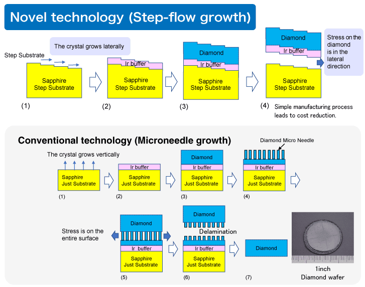
Here’s an in-depth look at each step involved in making diamond semiconductors:
1. Synthesis of Diamond
The synthesis of diamond suitable for semiconductor applications primarily uses two methods: High-Pressure High-Temperature (HPHT) and Chemical Vapor Deposition (CVD).
High-Pressure High-Temperature (HPHT) Method
Overview:
- The HPHT method simulates the natural formation conditions of diamond by applying high pressure (up to 5 GPa) and high temperature (up to 2000°C) to a carbon source.
- This method typically produces bulk diamond crystals.
Process:
- A carbon source, such as graphite, is placed in a press.
- The carbon source is subjected to high pressure and temperature in the presence of a metal catalyst, usually iron, nickel, or cobalt.
- Under these conditions, carbon atoms rearrange into a diamond structure.
Applications:
- HPHT diamonds are often used for industrial purposes, but their purity and quality make them less ideal for high-performance semiconductor applications compared to CVD diamonds.
Chemical Vapor Deposition (CVD) Method
Overview:
- CVD is the preferred method for producing high-quality diamond films for semiconductor applications.
- This method allows for precise control over the purity, thickness, and uniformity of the diamond layer.
Process:
- A gas mixture, typically methane (CH₄) and hydrogen (H₂), is introduced into a vacuum chamber.
- The gas is energized using microwaves or hot filaments to create a plasma.
- In the plasma, methane molecules break down, and carbon atoms are deposited onto a substrate, forming a diamond layer.
Advantages:
- CVD produces high-purity, single-crystal diamond films.
- It allows for the growth of diamond on various substrates, making it versatile for different applications.
2. Doping Diamond
Doping is the process of introducing impurities into the diamond lattice to modify its electrical properties, creating n-type or p-type semiconductors.
n-Type Doping
Process:
- n-Type doping involves introducing donor atoms, such as phosphorus or nitrogen, into the diamond lattice.
- These atoms have more valence electrons than carbon, providing extra free electrons for conduction.
Techniques:
- Ion Implantation: Phosphorus or nitrogen ions are accelerated and implanted into the diamond lattice. The sample is then annealed to repair damage and activate the dopants.
- In Situ Doping: During the CVD process, gases containing donor atoms are introduced, incorporating the dopants directly into the growing diamond film.
p-Type Doping
Process:
- p-Type doping involves introducing acceptor atoms, such as boron, into the diamond lattice.
- These atoms have fewer valence electrons than carbon, creating holes (positive charge carriers) in the lattice.
Techniques:
- In Situ Doping: During the CVD process, gases containing boron (e.g., diborane, B₂H₆) are introduced, allowing boron atoms to incorporate into the diamond lattice as it grows.
Challenges:
- Achieving uniform and controlled doping levels in diamond is challenging due to its robust crystal structure.
- p-Type doping with boron is relatively well-established, while n-type doping remains more complex and less mature.
3. Fabrication of Semiconductor Devices
Once high-quality, doped diamond layers are synthesized, they can be fabricated into semiconductor devices through a series of steps:
Patterning and Etching
Photolithography:
- A light-sensitive photoresist is applied to the diamond surface.
- UV light is used to transfer a pattern onto the photoresist, defining the areas to be etched.
Etching:
- Reactive ion etching (RIE) or other etching techniques are used to remove diamond material according to the pattern, creating the desired structures for electronic components.
Metal Contacts
Deposition:
- Metal contacts are deposited onto the patterned diamond surface to form electrical connections.
- Techniques such as sputtering, evaporation, or electroplating can be used to deposit metals like gold, platinum, or titanium.
Annealing:
- After deposition, the sample is often annealed to improve the contact quality and ensure good electrical conductivity.
Integration
Bonding:
- Diamond semiconductor devices can be bonded to other substrates or integrated into larger electronic systems.
- Techniques such as flip-chip bonding or wire bonding are used to connect diamond devices with other components.
Packaging:
- The devices are packaged to protect them from environmental factors and to facilitate their integration into electronic systems.
- Packaging involves encapsulating the device in a protective material and providing external connections for power and signal transmission.
Challenges and Future Directions
Cost:
- The high cost of synthesizing and processing diamond is a major challenge for widespread adoption.
- Ongoing research aims to develop cost-effective methods for diamond synthesis and device fabrication.
Scalability:
- Scaling up the production of high-quality diamond semiconductors to meet industrial demands is another significant challenge.
- Advances in CVD technology and doping techniques are critical for achieving scalable production.
Device Performance:
- Improving the performance and reliability of diamond semiconductor devices requires further optimization of doping processes, defect control, and integration techniques.
- Research focuses on enhancing the electronic properties of diamond through innovative material engineering and device design.
Also, Read: Trends in Welding Technology
Why Are Diamonds Used in the Semiconductor Industry?
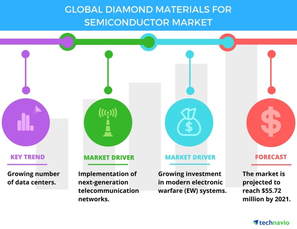
Diamonds are used in the semiconductor industry due to their exceptional properties that offer significant advantages over traditional semiconductor materials.
Key Reasons for Using Diamond:
- Thermal Management: Diamond’s high thermal conductivity enables efficient heat dissipation, crucial for high-power and high-frequency devices.
- Power Handling: The ability to operate at high voltages and currents makes diamond suitable for power electronics applications.
- Durability: Diamond’s resistance to radiation, chemical degradation, and extreme temperatures ensures long-term reliability and performance.
- High-Frequency Performance: Diamond’s high electron mobility supports faster signal processing and transmission in high-frequency applications.
The use of diamond in the semiconductor industry is driven by the need for materials that can enhance the performance, efficiency, and durability of electronic devices, particularly in demanding applications.
Also, Read: Trends in Electrical Cables
What Type of Semiconductor is a Diamond?
Diamond is classified as a wide bandgap semiconductor, which distinguishes it from traditional semiconductors like silicon.
Characteristics of Wide Bandgap Semiconductors:
- Wide Bandgap: Diamond’s bandgap of 5.5 eV is much wider than that of silicon (1.1 eV), allowing it to operate at higher temperatures and voltages.
- High Breakdown Voltage: The wide bandgap contributes to a high breakdown voltage, enabling diamond to handle high-power applications.
- High Thermal Conductivity: Wide bandgap semiconductors like diamond can efficiently dissipate heat, supporting stable operation in high-power and high-frequency devices.
Wide bandgap semiconductors, including diamond, are particularly advantageous for applications that require robust performance under extreme conditions.
What Are Diamond Photoconductive Semiconductor Switches?
Diamond photoconductive semiconductor switches (PCSS) are a type of electronic device that leverages the photoconductive properties of diamond to control the flow of electrical current. These switches are activated by light, typically in the ultraviolet (UV) spectrum, which induces changes in the electrical conductivity of the diamond material. Diamond PCSS are known for their high power handling capabilities, fast switching speeds, and robustness in harsh environments, making them ideal for various advanced applications.
Working Principle of Diamond PCSS
The operation of diamond photoconductive semiconductor switches relies on the photoconductivity phenomenon, where the conductivity of a material increases when exposed to light. Here’s how it works:
Photoconductivity
- Light Absorption: When diamond is exposed to light, photons with sufficient energy (typically UV light) are absorbed by the diamond material.
- Electron-Hole Pair Generation: The absorbed photons excite electrons from the valence band to the conduction band, creating electron-hole pairs. These charge carriers increase the electrical conductivity of the diamond.
- Conductive State: In the presence of light, the generated electron-hole pairs allow current to flow through the diamond PCSS. When the light is removed, the electron-hole pairs recombine, and the material returns to its non-conductive state.
Switching Mechanism
- Off State: In the absence of light, the diamond PCSS remains in a non-conductive state due to the wide bandgap of diamond, which minimizes the number of free charge carriers.
- On State: When a laser pulse or other light source illuminates the diamond PCSS, it generates sufficient electron-hole pairs to create a conductive path, allowing current to flow. The switch remains conductive as long as the light is present.
- Return to Off State: Once the light source is turned off, the electron-hole pairs quickly recombine, returning the switch to its non-conductive state.
Advantages of Diamond PCSS
Diamond photoconductive semiconductor switches offer several advantages over traditional PCSS made from materials like silicon or gallium arsenide:
High Power Handling
- Breakdown Voltage: Diamond has a high breakdown voltage, allowing diamond PCSS to handle very high voltages and currents without breaking down.
- Thermal Conductivity: The exceptional thermal conductivity of diamond helps dissipate heat efficiently, enabling the switch to handle high power levels without overheating.
Fast Switching Speeds
- Electron Mobility: Diamond’s high electron mobility allows for rapid generation and recombination of electron-hole pairs, resulting in very fast switching speeds.
- Wide Bandgap: The wide bandgap of diamond reduces the likelihood of thermal generation of charge carriers, ensuring that the switch remains off in the absence of light and turns on quickly when illuminated.
Robustness in Harsh Environments
- Radiation Resistance: Diamond’s resistance to radiation damage makes diamond PCSS suitable for applications in high-radiation environments, such as space and nuclear industries.
- Chemical Inertness: Diamond’s chemical inertness ensures that the switches remain stable and reliable even in corrosive environments.
Applications of Diamond PCSS
Diamond photoconductive semiconductor switches are used in various advanced applications that require high power handling, fast switching speeds, and robustness. Some notable applications include:
High-Power Electronics
- Pulsed Power Systems: Diamond PCSS are used in pulsed power systems, where they switch high voltages and currents rapidly to generate short, high-power pulses. These systems are used in applications such as radar, medical imaging, and particle accelerators.
- Laser Drivers: Diamond PCSS are used to drive high-power lasers, providing precise and rapid control over the laser pulses.
Microwave and RF Applications
- Microwave Generators: Diamond PCSS can switch high-frequency signals, making them suitable for generating microwave signals in communications and radar systems.
- RF Switches: The fast switching speeds and high power handling of diamond PCSS make them ideal for RF switching applications, where they can rapidly switch between different signal paths.
Space and Defense
- Radiation-Hardened Electronics: The radiation resistance of diamond PCSS makes them suitable for use in space and defense applications, where they can withstand high levels of radiation without degradation.
- Directed Energy Weapons: Diamond PCSS are used in directed energy weapons, where they control the flow of high-power electrical pulses to generate focused energy beams.
Challenges and Future Directions
While diamond PCSS offer significant advantages, there are also challenges to their widespread adoption:
High Cost
- Synthesis and Processing: The cost of synthesizing high-quality diamond and processing it into semiconductor devices is currently high. Efforts are ongoing to develop cost-effective methods for producing diamond PCSS.
Doping and Fabrication
- Doping Complexity: Achieving uniform and controlled doping in diamond is challenging, particularly for n-type doping. Advanced doping techniques are needed to improve the performance of diamond PCSS.
- Fabrication Techniques: Developing precise and scalable fabrication techniques for diamond PCSS is critical for their commercialization.
Market Adoption
- Limited Awareness: The potential of diamond PCSS is not yet widely recognized in all industries. Increased awareness and demonstration of their advantages are needed to drive market adoption.
Also, Read: Trends in Solar Energy, Systems and Products
Wide Band-Gap Semiconductor: How Good is Diamond?
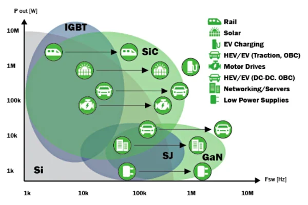
Wide band-gap semiconductors are materials with larger bandgaps compared to conventional semiconductors like silicon. These materials are capable of operating at higher voltages, temperatures, and frequencies, making them suitable for a variety of advanced applications. Diamond, with its exceptional properties, is considered one of the best wide band-gap semiconductors available. This article explores the advantages of diamond as a wide band-gap semiconductor, its applications, and how it compares to other wide band-gap materials.
Advantages of Diamond as a Wide Band-Gap Semiconductor
Diamond’s unique properties provide several advantages over other wide band-gap semiconductors such as silicon carbide (SiC) and gallium nitride (GaN).
1. Wide Bandgap
Diamond:
- Value: Diamond has a bandgap of 5.5 eV, which is significantly wider than that of silicon (1.1 eV), SiC (3.26 eV), and GaN (3.4 eV).
- Implications:
- High Temperature Operation: The wide bandgap allows diamond to operate at much higher temperatures without its electronic properties degrading.
- High Voltage Operation: A larger bandgap also enables diamond to withstand higher electric fields, making it ideal for high-power applications.
2. Thermal Conductivity
Diamond:
- Value: Diamond boasts a thermal conductivity of approximately 2200 W/m·K, the highest of any known material.
- Implications:
- Efficient Heat Dissipation: This property allows diamond to dissipate heat more effectively, preventing overheating and enabling stable operation in high-power devices.
Comparison:
- Silicon: About 150 W/m·K.
- SiC: Around 490 W/m·K.
- GaN: Approximately 130 W/m·K.
3. Breakdown Voltage
Diamond:
- Value: Diamond can withstand electric fields up to 10 MV/cm.
- Implications:
- High-Power Applications: The high breakdown voltage allows diamond to handle very high voltages and currents without breaking down, making it suitable for high-power electronics.
Comparison:
- Silicon: About 0.3 MV/cm.
- SiC: Around 2.8 MV/cm.
- GaN: Approximately 3.3 MV/cm.
4. Electron Mobility
Diamond:
- Value: Diamond has a high electron mobility, which allows for faster electron transport.
- Implications:
- High-Speed Devices: High electron mobility supports the development of faster and more efficient electronic devices, especially in high-frequency applications.
Comparison:
- Silicon: Lower than diamond.
- SiC and GaN: Both have good electron mobility but are generally lower than that of diamond.
5. Durability and Hardness
Diamond:
- Durability: Diamond is the hardest known material, making it highly resistant to physical wear and tear.
- Chemical Inertness: Diamond is chemically inert, providing resistance to corrosion.
- Radiation Resistance: Diamond is highly resistant to radiation damage, which is crucial for space and nuclear applications.
Implications:
- Harsh Environments: The superior durability and hardness of diamond make it ideal for use in harsh environments, ensuring long-term reliability and performance.
6. Thermal Stability
Diamond:
- Thermal Stability: Diamond can maintain its structural integrity and performance at very high temperatures.
Implications:
- Extreme Conditions: Diamond’s high thermal stability ensures consistent performance in extreme temperature conditions, making it ideal for applications that require high thermal tolerance.
Comparison with Other Wide Band-Gap Semiconductors
Silicon Carbide (SiC):
- Advantages: High thermal conductivity and breakdown voltage.
- Limitations: Lower thermal conductivity and electron mobility compared to diamond.
- Applications: Widely used in power electronics, especially in electric vehicles and renewable energy.
Gallium Nitride (GaN):
- Advantages: High electron mobility and breakdown voltage.
- Limitations: Lower thermal conductivity and wider bandgap than diamond.
- Applications: High-frequency and high-power applications, such as RF amplifiers and power electronics.
Overall, diamond’s properties as a wide bandgap semiconductor make it an excellent material for advanced electronic applications, providing superior performance and reliability.
Semiconductor Structure or Device Integrated with Diamond
Integrating diamond with other semiconductor materials and devices presents unique opportunities for enhancing performance and efficiency.
Types of Diamond Integration:
- Diamond-Coated Devices: Applying a diamond coating to semiconductor devices can improve thermal management and durability. For example, diamond-coated heat sinks can efficiently dissipate heat from high-power electronic components.
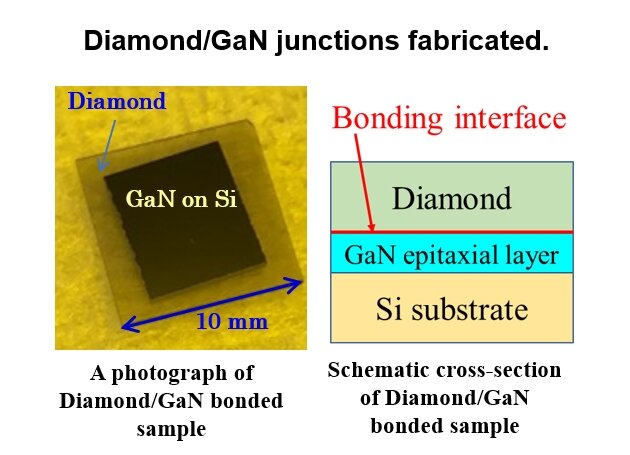
- Hybrid Devices: Combining diamond with other semiconductor materials, such as silicon or gallium nitride, can create hybrid devices that leverage the best properties of each material. These hybrid devices can offer improved performance, efficiency, and reliability.
- Monolithic Integration: Developing techniques for monolithic integration of diamond with semiconductor devices can lead to more compact and efficient electronic systems. This involves directly integrating diamond into the device structure, enhancing thermal management and performance.
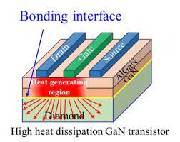
Applications of Diamond-Integrated Devices:
- Power Electronics: Diamond-integrated devices can handle higher power loads and operate more efficiently, making them ideal for power electronics applications.
- High-Frequency Systems: The high electron mobility of diamond supports faster signal processing, benefiting high-frequency systems such as telecommunications and radar.
- Advanced Sensors: Diamond’s robustness and sensitivity make it suitable for advanced sensor applications, including those in harsh environments.
Integrating diamond with other semiconductor materials and devices can significantly enhance their performance and open up new possibilities for advanced electronic systems.
The Chemistry of Diamond-Like Semiconductors
The chemistry of diamond-like semiconductors involves understanding the atomic structure and bonding characteristics that give these materials their unique properties.
Atomic Structure and Bonding:
- Carbon Lattice: Diamond is composed of carbon atoms arranged in a tetrahedral lattice structure. Each carbon atom forms strong covalent bonds with four neighboring carbon atoms, creating a rigid and durable structure.
- Hybridization: The carbon atoms in diamond are sp3 hybridized, which contributes to the material’s exceptional hardness and thermal conductivity.
- Impurities and Doping: Introducing impurities into the diamond lattice (doping) can modify its electronic properties. For example, boron doping creates p-type semiconductors, while phosphorus or nitrogen doping creates n-type semiconductors.
Synthesis and Modification:
- Chemical Vapor Deposition (CVD): CVD is the primary method for synthesizing diamond-like semiconductors. By controlling the gas composition, temperature, and pressure, high-quality diamond films can be deposited onto substrates.
- Surface Functionalization: Modifying the surface of diamond-like semiconductors can enhance their properties for specific applications. For example, hydrogen termination can improve the electronic properties of diamond surfaces, making them more suitable for electronic devices.
Understanding the chemistry of diamond-like semiconductors is crucial for developing advanced materials and devices that leverage the unique properties of diamond.
Diamond Semiconductor Performances in Power Electronics Applications
Diamond semiconductors offer significant performance advantages in power electronics applications, where efficient power handling and thermal management are crucial.
Key Performance Metrics:
- Thermal Conductivity: Diamond’s high thermal conductivity ensures efficient heat dissipation, preventing overheating and maintaining stable operation in high-power devices.
- Breakdown Voltage: The high breakdown voltage of diamond allows it to handle higher voltages, reducing the risk of device failure and improving reliability.
- Switching Speed: Diamond’s high electron mobility supports fast switching speeds, enhancing the performance of power electronic devices.
Applications in Power Electronics:
- Inverters and Converters: Diamond-based inverters and converters can operate more efficiently and handle higher power loads than traditional silicon-based devices. This is particularly beneficial in renewable energy systems and electric vehicles.
- Power Supplies: Diamond semiconductors can improve the efficiency and reliability of power supplies, supporting applications that require stable and high-quality power.
- Motor Drives: Diamond-based motor drives offer improved performance and efficiency, reducing energy consumption and enhancing the reliability of industrial machinery.
The superior performance of diamond semiconductors in power electronics applications makes them a valuable choice for enhancing the efficiency, reliability, and performance of power systems.
Diamond Semiconductor Companies
Several companies are leading the development and commercialization of diamond semiconductor technology. These companies are at the forefront of research, innovation, and application, driving advancements in various industries, including electronics, power, telecommunications, and more. Below are some of the key players in the diamond semiconductor industry:
1. Element Six
Overview: Element Six, a member of the De Beers Group, is one of the world’s leading producers of synthetic diamond supermaterials. The company is known for its expertise in producing high-quality diamond materials for industrial and electronic applications.
Key Contributions:
- High-Performance Materials: Element Six develops synthetic diamonds with exceptional purity and quality, tailored for semiconductor applications.
- Innovation in Synthesis: The company utilizes advanced chemical vapor deposition (CVD) techniques to produce diamond materials with precise control over their properties.
- Applications: Element Six’s diamond semiconductors are used in power electronics, thermal management systems, and high-frequency devices.
Notable Projects:
- Development of diamond-based heat spreaders for high-power electronic devices.
- Research on diamond semiconductors for use in next-generation power grids and electric vehicles.
Overview: AKHAN Semiconductor specializes in diamond-based electronics, focusing on leveraging the superior properties of diamond to enhance the performance of semiconductor devices.
Key Contributions:
- MIRAJ Diamond™ Technology: AKHAN’s proprietary technology involves the integration of diamond materials into semiconductor devices, significantly improving their thermal and electrical performance.
- Product Portfolio: The company’s product line includes diamond-based transistors, diodes, and other semiconductor components.
- Research and Development: AKHAN is actively engaged in developing diamond semiconductors for applications in high-power electronics, aerospace, and defense.
Notable Projects:
- Collaboration with major aerospace and defense contractors to develop radiation-hardened diamond semiconductor devices.
- Development of diamond-based power electronics for electric vehicles and renewable energy systems.
Overview: II-VI Incorporated is a global leader in engineered materials and optoelectronic components. The company has expanded its portfolio to include diamond materials for semiconductor applications.
Key Contributions:
- Advanced Materials: II-VI produces high-quality diamond materials for use in high-power and high-frequency semiconductor devices.
- Integration with Existing Technologies: The company focuses on integrating diamond semiconductors with other advanced materials to create hybrid devices with superior performance.
- Applications: II-VI’s diamond semiconductors are used in telecommunications, power electronics, and thermal management systems.
Notable Projects:
- Development of diamond-based RF and microwave components for telecommunications.
- Research on diamond heat spreaders for high-performance computing and electronic devices.
4. Advanced Diamond Technologies (ADT)
Overview: Advanced Diamond Technologies (ADT) is a pioneer in the development of diamond films and coatings for a variety of industrial and electronic applications.
Key Contributions:
- UNCD® Technology: ADT’s Ultrananocrystalline Diamond (UNCD) technology produces diamond films with nanometer-scale grain sizes, offering exceptional properties for semiconductor applications.
- Diverse Applications: ADT’s diamond films are used in sensors, electronic devices, and industrial tools.
- Research and Development: The company focuses on advancing diamond film technology to improve the performance and reliability of semiconductor devices.
Notable Projects:
- Development of diamond-coated sensors for harsh environments.
- Research on diamond films for use in advanced optoelectronic devices.
Overview: Blue Wave Semiconductor is an innovative company dedicated to developing diamond-based solutions for advanced electronics and power systems.
Key Contributions:
- Diamond-Based Solutions: Blue Wave focuses on creating diamond semiconductors that offer superior thermal management and electrical performance.
- Product Development: The company develops diamond-based transistors, diodes, and power electronics components.
- Research Focus: Blue Wave is involved in cutting-edge research to optimize diamond synthesis and integration techniques.
Notable Projects:
- Collaboration with academic institutions to advance diamond semiconductor technology.
- Development of diamond-based power electronics for renewable energy applications.
6. Sumitomo Electric Industries
Overview: Sumitomo Electric Industries is a major player in the electronics and materials industry, with a strong focus on developing diamond semiconductors for various applications.
Key Contributions:
- Advanced Materials: Sumitomo produces high-quality diamond substrates and components for semiconductor devices.
- Innovation in Electronics: The company focuses on leveraging diamond’s properties to enhance the performance of power electronics and high-frequency devices.
- Global Presence: Sumitomo’s diamond semiconductors are used in telecommunications, automotive, and industrial applications worldwide.
Notable Projects:
- Development of diamond-based high-frequency transistors for 5G technology.
- Research on diamond semiconductors for electric vehicle power control units.
7. SP3 Diamond Technologies
Overview: SP3 Diamond Technologies specializes in the production of diamond coatings and materials for industrial and electronic applications.
Key Contributions:
- CVD Diamond Technology: SP3 uses chemical vapor deposition to produce high-quality diamond coatings with excellent thermal and electrical properties.
- Diverse Applications: The company’s diamond materials are used in cutting tools, thermal management systems, and semiconductor devices.
- Research and Innovation: SP3 focuses on advancing CVD techniques to improve the quality and performance of diamond semiconductors.
Notable Projects:
- Development of diamond-coated heat sinks for high-power electronics.
- Research on diamond semiconductors for next-generation power electronics.
Diamond Semiconductor Price
The cost of diamond semiconductors is a critical factor influencing their adoption and commercialization. While diamond offers numerous advantages over traditional semiconductor materials such as silicon, its higher cost has been a significant barrier to widespread use. Understanding the factors that contribute to the price of diamond semiconductors is essential for evaluating their potential in various applications.
Factors Affecting Diamond Semiconductor Price
Several factors influence the cost of diamond semiconductors, including the synthesis method, quality and purity of the diamond material, doping and processing techniques, and market demand.
1. Synthesis Method
High-Pressure High-Temperature (HPHT) Method:
- Overview: The HPHT method mimics the natural formation of diamonds by applying high pressure and high temperature to a carbon source.
- Cost Implications: While suitable for producing bulk diamond crystals, HPHT diamonds are typically less pure and more costly when high purity is required for semiconductor applications.
Chemical Vapor Deposition (CVD) Method:
- Overview: The CVD method involves introducing a gas mixture containing carbon (usually methane) into a chamber, where it decomposes and deposits carbon atoms onto a substrate, forming a diamond film.
- Cost Implications: CVD is the preferred method for synthesizing diamond for semiconductor applications due to its ability to produce high-purity, single-crystal diamond films. However, the CVD process is expensive and requires precise control over the deposition parameters, contributing to the high cost.
2. Quality and Purity
High-Purity Diamond:
- Overview: The performance of diamond semiconductors is highly dependent on the purity of the diamond material. High-purity, single-crystal diamonds are necessary for optimal electronic properties.
- Cost Implications: Achieving high purity involves advanced synthesis techniques and stringent quality control, increasing the cost of the final product.
Impurities and Defects:
- Overview: The presence of impurities and defects in the diamond lattice can significantly degrade the performance of semiconductor devices.
- Cost Implications: Reducing impurities and defects requires sophisticated processing and quality assurance measures, which add to the overall cost.
3. Doping and Processing
Doping Techniques:
- Overview: Doping involves introducing specific elements into the diamond lattice to modify its electronic properties, creating n-type or p-type semiconductors.
- Cost Implications: The process of doping diamond is complex and requires advanced techniques to achieve uniform and controllable doping levels. This complexity adds to the manufacturing cost.
Processing and Fabrication:
- Overview: Fabricating diamond semiconductor devices involves several steps, including patterning, etching, and depositing metal contacts.
- Cost Implications: The precision required in these processes and the need for specialized equipment contribute to the high cost of diamond semiconductor production.
4. Market Demand and Scale of Production
Current Market Demand:
- Overview: The demand for diamond semiconductors is currently limited to specialized applications where their superior properties justify the higher cost.
- Cost Implications: Limited demand and small-scale production mean that economies of scale have not been realized, keeping prices high.
Future Market Potential:
- Overview: As research progresses and new applications are developed, the demand for diamond semiconductors is expected to grow.
- Cost Implications: Increased demand and larger-scale production could lead to cost reductions over time through economies of scale and improved manufacturing techniques.
Current Market Prices
The price of diamond semiconductors can vary widely based on the factors discussed above. Here are some approximate price ranges for different types of diamond materials used in semiconductor applications:
Bulk Diamond:
- Price Range: The price of bulk diamond materials varies widely depending on quality and size. High-quality single-crystal diamond wafers can cost several thousand dollars per carat. For example, high-purity diamond wafers suitable for electronic applications can range from $2,000 to $10,000 per carat.
Diamond Films:
- Price Range: The cost of diamond films produced by CVD is influenced by the thickness, quality, and substrate material. Prices can range from a few hundred to several thousand dollars per square centimeter. For instance, a high-quality CVD diamond film of a few micrometers thickness can cost around $500 to $2,000 per square centimeter.
Doped Diamond:
- Price Range: The cost of doped diamond materials depends on the doping technique and the desired electronic properties. Doped diamond for semiconductor applications can be significantly more expensive due to the complexities involved in achieving uniform doping. Prices can range from $5,000 to $20,000 per carat for high-purity, uniformly doped diamond materials.
Efforts to Reduce Costs
Several strategies are being explored to reduce the cost of diamond semiconductors and make them more competitive with traditional materials like silicon:
1. Improved Synthesis Techniques:
- Advancements in CVD technology are aimed at increasing the deposition rate and improving the uniformity of diamond films, which could lower production costs.
2. Economies of Scale:
- As the demand for diamond semiconductors grows, larger-scale production could help reduce costs through economies of scale.
3. Hybrid Materials:
- Integrating diamond with other semiconductor materials to create hybrid devices can leverage the best properties of each material while potentially reducing overall costs.
4. Government and Industry Support:
- Increased funding and support from governments and industry stakeholders for research and development can accelerate advancements in diamond semiconductor technology, leading to cost reductions.
As research and development continue and new applications emerge, the cost of diamond semiconductors is expected to decrease, making them more accessible for a wider range of industries and applications.
Band Structure of Diamond Semiconductors
Band Structure of Diamond Semiconductors
The band structure of a semiconductor determines its electronic properties, such as electrical conductivity, bandgap energy, and electron mobility. Diamond, with its unique atomic structure, exhibits exceptional electronic properties that make it an attractive material for high-performance semiconductor applications. Understanding the band structure of diamond is essential for optimizing its use in various electronic devices.
Understanding the Band Structure
The band structure of a semiconductor describes the relationship between the energy levels of electrons and their momentum. It consists of two main bands:
- Valence Band: The energy band that holds the electrons bound to atoms. It is fully occupied by electrons at absolute zero temperature.
- Conduction Band: The energy band where electrons can move freely, contributing to electrical conductivity. It is typically empty at absolute zero temperature.
The energy gap between the valence band and the conduction band is known as the bandgap. The bandgap determines the electrical conductivity and other electronic properties of the semiconductor.
Key Characteristics of Diamond’s Band Structure
Wide Bandgap
- Value: Diamond has a wide bandgap of 5.5 eV, which is much larger than that of silicon (1.1 eV).
- Implications:
- High Temperature Operation: The wide bandgap allows diamond to operate at much higher temperatures without its electronic properties degrading, making it ideal for high-temperature applications.
- High Voltage Operation: The large bandgap also enables diamond to withstand high electric fields, making it suitable for high-power electronic devices.
Valence and Conduction Bands
- Valence Band: In diamond, the valence band is fully occupied by electrons at absolute zero temperature. The electrons in this band are bound to the carbon atoms within the crystal lattice.
- Conduction Band: The conduction band in diamond is typically empty at absolute zero temperature. Electrons need to gain sufficient energy (equal to or greater than the bandgap) to move from the valence band to the conduction band, where they can contribute to electrical conductivity.
High Electron and Hole Mobility
- Electron Mobility: Diamond exhibits high electron mobility, meaning that electrons can move through the conduction band with minimal resistance. This property is crucial for high-speed electronic devices.
- Hole Mobility: The mobility of holes (the absence of an electron in the valence band) in diamond is also high, which enhances the overall conductivity and performance of p-type diamond semiconductors.
Low Intrinsic Carrier Concentration
- Overview: Due to its wide bandgap, diamond has a very low intrinsic carrier concentration at room temperature. This means that the number of free electrons and holes in an undoped diamond semiconductor is extremely low.
- Implications: The low intrinsic carrier concentration reduces leakage currents in electronic devices, making diamond semiconductors highly efficient and reliable for power electronics and other applications requiring low standby power consumption.
Implications for Electronic Devices
High Temperature and High Power Applications
- Thermal Stability: The wide bandgap and high thermal conductivity of diamond allow electronic devices to operate reliably at high temperatures. This makes diamond semiconductors ideal for applications in aerospace, automotive, and industrial environments where thermal management is critical.
- Power Electronics: Diamond’s ability to handle high voltages and currents without breaking down makes it suitable for power electronics, such as power inverters, converters, and power control units in electric vehicles and renewable energy systems.
High-Frequency Devices
- Telecommunications: The high electron mobility in diamond semiconductors supports the development of high-frequency transistors and other components for telecommunications. These devices can operate at higher speeds, enabling faster data transmission and more efficient signal processing.
- RF and Microwave Applications: Diamond semiconductors are also used in RF (radio frequency) and microwave applications, where they provide superior performance compared to traditional materials like silicon and gallium nitride.
Radiation-Hardened Electronics
- Space and Defense: Diamond’s wide bandgap and robust atomic structure make it highly resistant to radiation damage. This property is particularly valuable for space and defense applications, where electronic components must withstand high levels of radiation and extreme environmental conditions.
Optoelectronics
- Light Emitting Diodes (LEDs): Diamond’s wide bandgap allows it to emit light in the ultraviolet (UV) range, making it suitable for UV LEDs. These LEDs have applications in sterilization, medical devices, and advanced lighting systems.
- Photodetectors: Diamond-based photodetectors can operate in harsh environments and provide high sensitivity and fast response times, beneficial for imaging and sensing applications.
Research and Developments in Diamond Band Structure
Researchers are continually exploring ways to optimize the band structure of diamond for various semiconductor applications. This includes:
- Doping Techniques: Advanced doping methods to create n-type and p-type diamond semiconductors with controlled electronic properties.
- Defect Engineering: Techniques to minimize defects in the diamond lattice that can affect its electronic performance.
- Hybrid Structures: Combining diamond with other materials to create hybrid semiconductor devices that leverage the unique properties of each material.
Conclusion
Diamond semiconductors represent a significant advancement in the field of electronics, offering unparalleled thermal management, power handling, efficiency, and durability. As research and development continue to progress, diamond semiconductors are poised to transform various industries and applications. From high-power electronics to advanced optoelectronics and quantum computing, the potential of diamond technology is vast, driving innovation and performance to new heights. The future of electronics looks bright with the promise of diamond semiconductors leading the way.
About Right Patents
Right Patents is a Reliable and Leading Patent Services Provider Company in the United States. We provide Top-Quality and Most Trusted Patent Drawing Services, Patentability Searches, Invalidity Searches, FTO Searches, and Patent Landscapes.
